
3
12
Series of Decoders
1
December 13, 1999
General Description
The 3
12
decoders are a series of CMOS LSIs for
remote control system applications. They are
paired with 3
12
series of encoders. For proper
operation a pair of encoder/decoder with the
same number of address and data format
should be selected (refer to the encoder/decoder
cross reference tables).
The 3
12
series of decoders receive serial address
and data from its corredponding series of
encoders that are transmitted by a carrier us-
ing an RF or an IR transmission medium. Then
it compares the serial input information twice
continuously with its local address. If no errors
or unmatched codes are encountered, the input
data codes are decoded and transferred to the
output pins. The VT pin also goes high to indi-
cate a valid transmission.
The 3
12
series of decoders are capable of decod-
ing 12 bits of information that consists of N bits
of address and 12-N bits of data. To meet vari-
ous applications they are arranged to provide a
number of data pins ranging from 0 to 4 and an
address pin ranging from 8 to 12. Thus, various
combinations of address/data number are
available in different packages.
Features
·
Operating voltage: 2.4V~12V
·
Low power and high noise immunity CMOS
technology
·
Low standby current
·
Capable of decoding 12 bits of information
·
Pair with HoltekĒs 3
12
series of encoders
·
8~12 address pins
·
0~4 data pins
·
Trinary address setting
·
Received data are checked two times
·
Built-in oscillator needs only 5% resistor
·
VT goes high during a valid transmission
·
Easy interface with an RF or an infrared
transmission medium
·
Minimal external components
·
Package information: refer to Selection
Table
Applications
·
Burglar alarm system
·
Smoke and fire alarm system
·
Garage door controllers
·
Car door controllers
·
Car alarm system
·
Security system
·
Cordless telephones
·
Other remote control systems

Selection Table
Function Address
No.
Data
VT
Oscillator
Trigger
Package
Part No.
No.
Type
HT6030
12
0
ū
Ö
RC oscillator DIN active ēHiē 18 DIP/20 SOP
HT6032
10
2
L
Ö
RC oscillator DIN active ēHiē 18 DIP/20 SOP
HT6034
8
4
L
Ö
RC oscillator DIN active ēHiē 18 DIP/20 SOP
Note: Data type: L stands for latch type data output.
VT can be used as a momentary data output.
Block Diagram
Note: The address/data pins are available in various combinations (refer to the address/data table).
3
12
Series of Decoders
2
December 13, 1999
D a t a S h i f t
R e g i s t e r
O s c i l l a t o r
B u f f e r
S y n c . D e t e c t o r
D i v i d e r
C o m p a r a t o r
C o m p a r a t o r
B u f f e r
T r a n s m i s s i o n G a t e C i r c u i t
D a t a D e t e c t o r
C o n t r o l L o g i c
V D D
V S S
V T
D a t a
L a t c h C i r c u i t
A d d r e s s
O S C 1
O S C 2
D I N
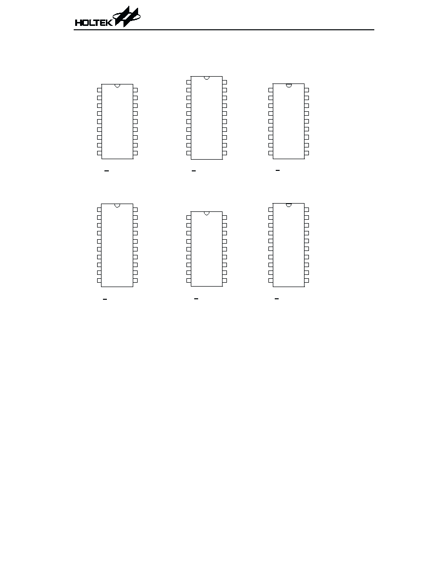
Pin Assignment
3
12
Series of Decoders
3
December 13, 1999
1 0 - A d d r e s s
2 - D a t a
8 - A d d r e s s
4 - D a t a
A 0
A 1
A 2
A 3
A 4
A 5
A 6
A 7
V S S
V D D
V T
O S C 2
O S C 1
D I N
D 1 1
D 1 0
A 9
A 8
1
2
3
4
5
6
7
8
9
1 8
1 7
1 6
1 5
1 4
1 3
1 2
1 1
1 0
8 - A d d r e s s
4 - D a t a
A 0
A 1
A 2
A 3
A 4
A 5
A 6
A 7
V S S
V D D
V T
O S C 2
O S C 1
D I N
D 1 1
D 1 0
D 9
D 8
1
2
3
4
5
6
7
8
9
1 8
1 7
1 6
1 5
1 4
1 3
1 2
1 1
1 0
1
2
3
4
5
6
7
8
9
1 0
2 0
1 9
1 8
1 7
1 6
1 5
1 4
1 3
1 2
1 1
N C
V D D
V T
O S C 2
O S C 1
D I N
D 1 1
D 1 0
D 9
D 8
N C
A 0
A 1
A 2
A 3
A 4
A 5
A 6
A 7
V S S
1 0 - A d d r e s s
2 - D a t a
1
2
3
4
5
6
7
8
9
1 0
2 0
1 9
1 8
1 7
1 6
1 5
1 4
1 3
1 2
1 1
N C
V D D
V T
O S C 2
O S C 1
D I N
D 1 1
D 1 0
A 9
A 8
N C
A 0
A 1
A 2
A 3
A 4
A 5
A 6
A 7
V S S
H T 6 0 3 2
1 8 D I P
H T 6 0 3 2
2 0 S O P
H T 6 0 3 4
1 8 D I P
H T 6 0 3 4
2 0 S O P
1 2 - A d d r e s s
0 - D a t a
1
2
3
4
5
6
7
8
9
1 0
2 0
1 9
1 8
1 7
1 6
1 5
1 4
1 3
1 2
1 1
N C
V D D
V T
O S C 2
O S C 1
D I N
A 1 1
A 1 0
A 9
A 8
N C
A 0
A 1
A 2
A 3
A 4
A 5
A 6
A 7
V S S
1 2 - A d d r e s s
0 - D a t a
A 0
A 1
A 2
A 3
A 4
A 5
A 6
A 7
V S S
V D D
V T
O S C 2
O S C 1
D I N
A 1 1
A 1 0
A 9
A 8
1
2
3
4
5
6
7
8
9
1 8
1 7
1 6
1 5
1 4
1 3
1 2
1 1
1 0
H T 6 0 3 0
1 8 D I P
H T 6 0 3 0
2 0 S O P
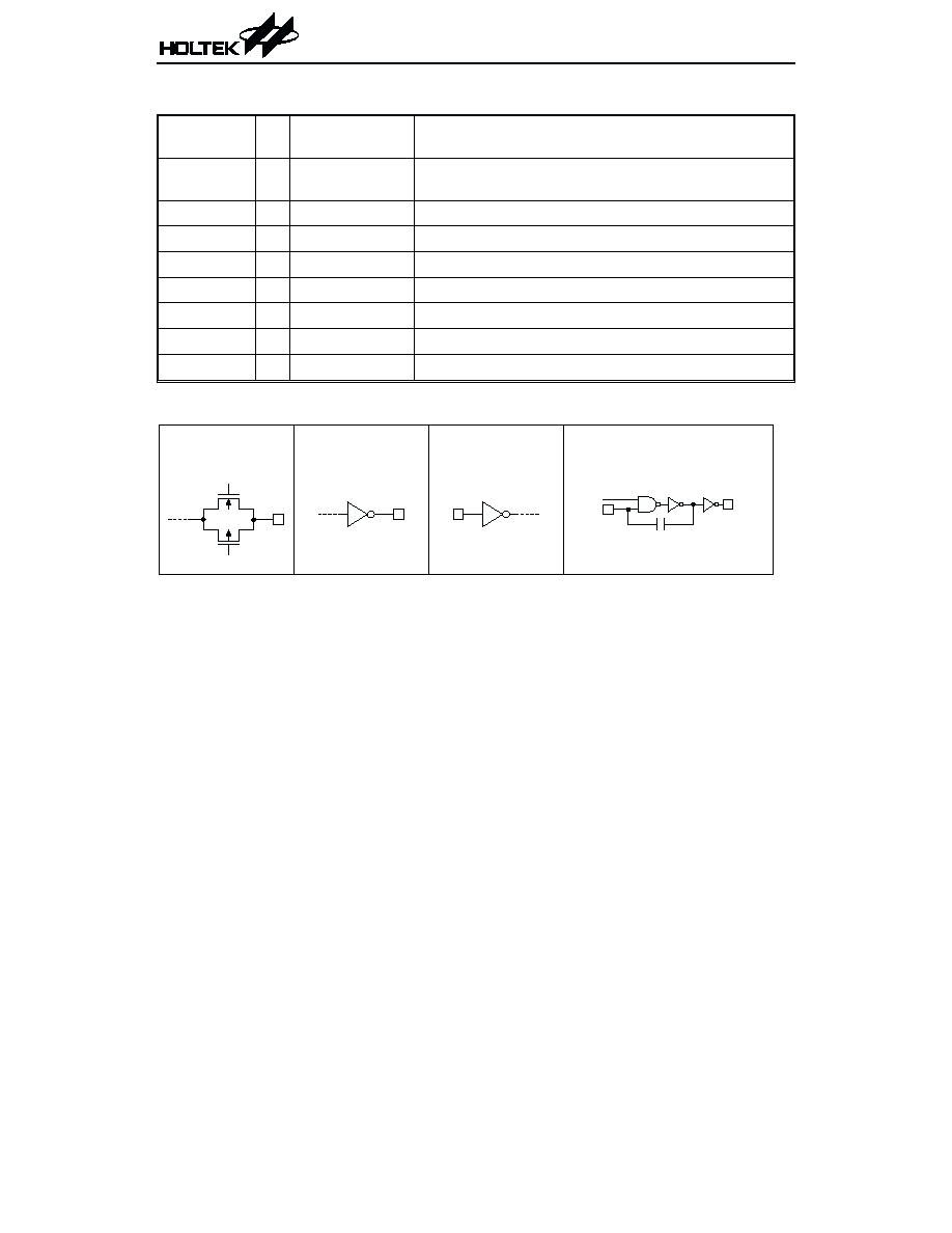
Pin Description
Pin Name
I/O
Internal
Connection
Description
A0~A11
I
TRANSMISSION
GATE
Input pins for address A0~A11 setting
They can be externally set to VDD, VSS, or left open.
D8~D11
O
CMOS OUT
Output data pins
DIN
I
CMOS IN
Serial data input pin
VT
O
CMOS OUT
Valid transmission, active high
OSC1
I
OSCILLATOR
Oscillator input pin
OSC2
O
OSCILLATOR
Oscillator output pin
VSS
ū
ū
Negative power supply, ground
VDD
ū
ū
Positive power supply
Approximate internal connections
Absolute Maximum Ratings
Supply Voltage...............................-0.3V to 13V
Storage Temperature.................-50°C to 125°C
Input Voltage....................V
SS
-0.3 to V
DD
+0.3V
Operating Temperature ..............-20°C to 75°C
Note: These are stress ratings only. Stresses exceeding the range specified under ēAbsolute Maxi-
mum Ratingsē may cause substantial damage to the device. Functional operation of this device
at other conditions beyond those listed in the specification is not implied and prolonged expo-
sure to extreme conditions may affect device reliability.
3
12
Series of Decoders
4
December 13, 1999
T R A N S M I S S I O N
G A T E
C M O S I N
O S C I L L A T O R
O S C 2
C M O S O U T
O S C 1
E N
