Document Outline
- ţ˙
- ţ˙
- ţ˙
- ţ˙
- ţ˙
- ţ˙
- ţ˙
- ţ˙
- ţ˙
- ţ˙
- ţ˙
3
12
Series of Encoders
Selection Table
Function Address
No.
Address/
Data No.
Data
No.
Oscillator
Trigger
LED
Indicator
Package
Part No.
HT6010
8
4
0
RC oscillator
TE
No
18/20 DIP
20 SOP
HT6012
10
0
2
RC oscillator
D10~D11
Yes
18 DIP/20 SOP
HT6014
8
0
4
RC oscillator
D8~D11
Yes
18 DIP/20 SOP
Note: Address/Data represents addressable pins or data according to the requirements of decoders.
1
December 13, 1999
General Description
The 3
12
encoders are a series of CMOS LSIs for
remote control system applications. They are ca-
pable of encoding 12 bits of information which
consists of N address bits and 12-N data bits.
Each address/data input is externally trinary
programmableifbondedout.Theyareotherwise
set floating internally. Various packages of the
3
12
encoders offer flexible combinations of
programmable address/data which meet vari-
ous applications. The programmable ad-
dress/dataistransmittedtogetherwiththeheader
bitsviaanRForaninfraredtransmissionmedium
upon receipt of a trigger signal. A TE (HT6010) or
a DATA (HT6012/HT6014) trigger can be se-
lectedforapplicationflexibility.
Features
·
Operating voltage: 2.4V~12V
·
Low power and high noise immunity CMOS
technology
·
Low standby current
·
Minimum transmission word
-
Four words for TE trigger
-
One word for Data trigger
·
Built-in oscillator needs only 5% resistor
·
Easy interface with an RF or an infrared
transmission medium
·
Minimal external components
·
Package information: refer to Selection
Table
Applications
·
Burglar alarm system
·
Smoke and fire alarm system
·
Garage door controllers
·
Car alarm system
·
Security system
·
Cordless telephones
·
Other remote control systems
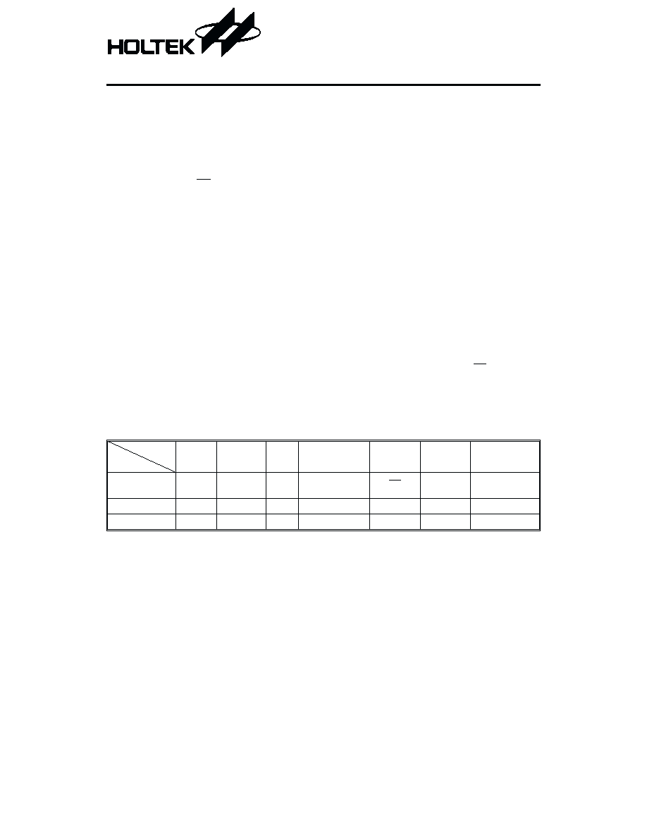
Block Diagram
TE trigger
HT6010
DATA trigger
HT6012/HT6014
Note: The address/data pins are available in various combinations (refer to the address/data table).
3
12
Series of Encoders
2
December 13, 1999
T E
O s c i l l a t o r
¸ 3 D i v i d e r
O S C 1
O S C 2
V D D
V S S
1 2
T r a n s m i s s i o n
G a t e C i r c u i t
¸ 1 2 C o u n t e r
a n d 1 o f 1 2
D e c o d e r s
T r i n a r y
D e t e c t o r
A 0
A 7
A D 8 A D 1 1
D O U T
D a t a S e l e c t
a n d B u f f e r
S y n c .
C i r c u i t
A d d r e s s
D a t a
O s c i l l a t o r
¸ 3 D i v i d e r
O S C 1
O S C 2
V D D
V S S
1 2
T r a n s m i s s i o n
G a t e C i r c u i t
¸ 1 2 C o u n t e r
a n d 1 o f 1 2
D e c o d e r s
T r i n a r y
D e t e c t o r
D O U T
D a t a S e l e c t
a n d B u f f e r
S y n c .
C i r c u i t
L E D C i r c u i t
L E D

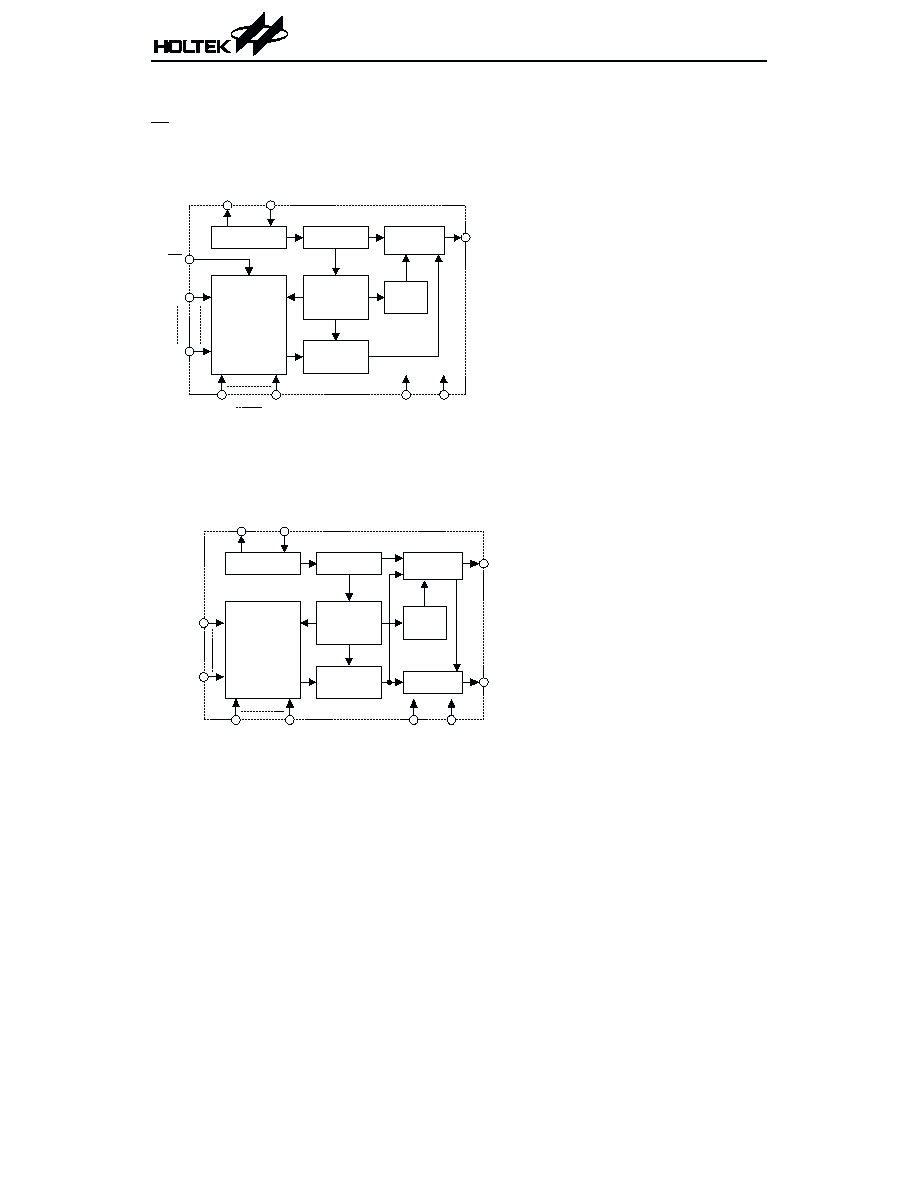
Pin Assignment
3
12
Series of Encoders
3
December 13, 1999
T E t r i g g e r t y p e
8 - A d d r e s s
4 - A d d r e s s / D a t a
A 0
A 1
A 2
A 3
A 4
A 5
A 6
A 7
V S S
V D D
D O U T
O S C 2
O S C 1
T E
A D 1 1
A D 1 0
A D 9
A D 8
N C
A 0
A 1
A 2
A 3
A 4
A 5
A 6
A 7
V S S
8 - A d d r e s s
4 - A d d r e s s / D a t a
D A T A t r i g g e r t y p e
8 - A d d r e s s
4 - D a t a
A 0
A 1
A 2
A 3
A 4
A 5
A 6
A 7
V S S
V D D
D O U T
O S C 2
O S C 1
L E D
D 1 1
D 1 0
D 9
D 8
1
2
3
4
5
6
7
8
9
1 8
1 7
1 6
1 5
1 4
1 3
1 2
1 1
1 0
N C
A 0
A 1
A 2
A 3
A 4
A 5
A 6
A 7
V S S
1 0 - A d d r e s s
2 - D a t a
H T 6 0 1 4
2 0 S O P
N C
A 0
A 1
A 2
A 3
A 4
A 5
A 6
A 7
V S S
8 - A d d r e s s
4 - D a t a
N C
V D D
D O U T
O S C 2
O S C 1
L E D
D 1 1
D 1 0
D 9
D 8
N C
V D D
D O U T
O S C 2
O S C 1
L E D
D 1 1
D 1 0
A 9
A 8
1 0 - A d d r e s s
2 - D a t a
A 0
A 1
A 2
A 3
A 4
A 5
A 6
A 7
V S S
V D D
D O U T
O S C 2
O S C 1
L E D
D 1 1
D 1 0
A 9
A 8
1
2
3
4
5
6
7
8
9
1 8
1 7
1 6
1 5
1 4
1 3
1 2
1 1
1 0
N C
V D D
D O U T
O S C 2
O S C 1
T E
A D 1 1
A D 1 0
A D 9
A D 8
2 0
1 9
1 8
1 7
1 6
1 5
1 4
1 3
1 2
1 1
1
2
3
4
5
6
7
8
9
1 0
2 0
1 9
1 8
1 7
1 6
1 5
1 4
1 3
1 2
1 1
1
2
3
4
5
6
7
8
9
1 0
2 0
1 9
1 8
1 7
1 6
1 5
1 4
1 3
1 2
1 1
1
2
3
4
5
6
7
8
9
1 0
1 8
1 7
1 6
1 5
1 4
1 3
1 2
1 1
1 0
1
2
3
4
5
6
7
8
9
H T 6 0 1 0
1 8 D I P
H T 6 0 1 0
2 0 D I P / S O P
H T 6 0 1 2
1 8 D I P
H T 6 0 1 2
2 0 S O P
H T 6 0 1 4
1 8 D I P

Pin Description
Pin Name I/O
Internal
Connection
Description
A0~A9
I TRANSMISSION
GATE
Input pins for address A0~A9 setting
They can be externally set to VDD or VSS or left open.
AD8~AD11
I TRANSMISSION
GATE
Input pins for address/data (AD8~AD11) setting
They can be externally set to VDD or VSS or left open.
D8~D11
I
CMOS IN
Pull-high
Input pins for data (D8~D11) setting and transmission en-
able (active low)
They can be externally set to VSS or left open (see Note).
DOUT
O
CMOS OUT
Encoder data serial transmission output
LED
O
NMOS OUT
Transmission enable indicator, active low
TE
I
CMOS IN
Pull-high
Transmission enable, active low (see Note)
OSC1
I
OSCILLATOR
Oscillator input pin
OSC2
O
OSCILLATOR
Oscillator output pin
VSS
ľ
ľ
Negative power supply, ground
VDD
ľ
ľ
Positive power supply
Note: D8~D11 are data input and transmission enable pins of the HT6012/HT6014.
TE is the transmission enable pin of the HT6010.
Approximate internal connections
3
12
Series of Encoders
4
December 13, 1999
T R A N S M I S S I O N
G A T E
C M O S I N
P u l l - h i g h
C M O S O U T
N M O S O U T
O S C I L L A T O R
O S C 1
O S C 2
E N

Absolute Maximum Ratings
Supply Voltage...............................-0.3V to 13V
Storage Temperature.................-50°C to 125°C
Input Voltage....................V
SS
-0.3 to V
DD
+0.3V
Operating Temperature ..............-20°C to 75°C
Note: These are stress ratings only. Stresses exceeding the range specified under ˛Absolute Maxi-
mum Ratings˛ may cause substantial damage to the device. Functional operation of this device
at other conditions beyond those listed in the specification is not implied and prolonged expo-
sure to extreme conditions may affect device reliability.
Electrical Characteristics
Ta=25°C
Symbol
Parameter
Test Conditions
Min.
Typ.
Max. Unit
V
DD
Conditions
V
DD
Operating Voltage
ľ
ľ
2.4
5
12
V
I
STB
Standby Current
3V
Oscillator stops
ľ
0.1
1
mA
12V
ľ
2
4
mA
I
DD
Operating Current
3V
No load
f
OSC
=3kHz
ľ
250
500
mA
12V
ľ
600
1200
mA
I
LED
LED Sink Current
5V
V
LED
=0.5V
1.5
3
ľ
mA
I
DOUT
Output Drive Current
5V
V
OH
=0.9V
DD
(Source)
-0.6
-1.2
ľ
mA
5V
V
OL
=0.1V
DD
(Sink)
0.6
1.2
ľ
mA
V
IH
˛H˛ Input Voltage
ľ
ľ
0.8V
DD
ľ
V
DD
V
V
IL
˛L˛ Input Voltage
ľ
ľ
0
ľ
0.2V
DD
V
f
OSC
Oscillator Frequency
5V
R
OSC
=1MW
ľ
3
ľ
kHz
R
TE
TE Pull-high Resistance
5V
V
TE
=0V
ľ
1.5
3
MW
R
DATA
D8~D11 Pull-high
Resistance
5V
V
DATA
=0V
ľ
1.5
3
MW
3
12
Series of Encoders
5
December 13, 1999