HM9264B Series
64 k SRAM (8-kword
Î
8-bit)
ADE-203-618C (Z)
Rev. 3.0
Nov. 1997
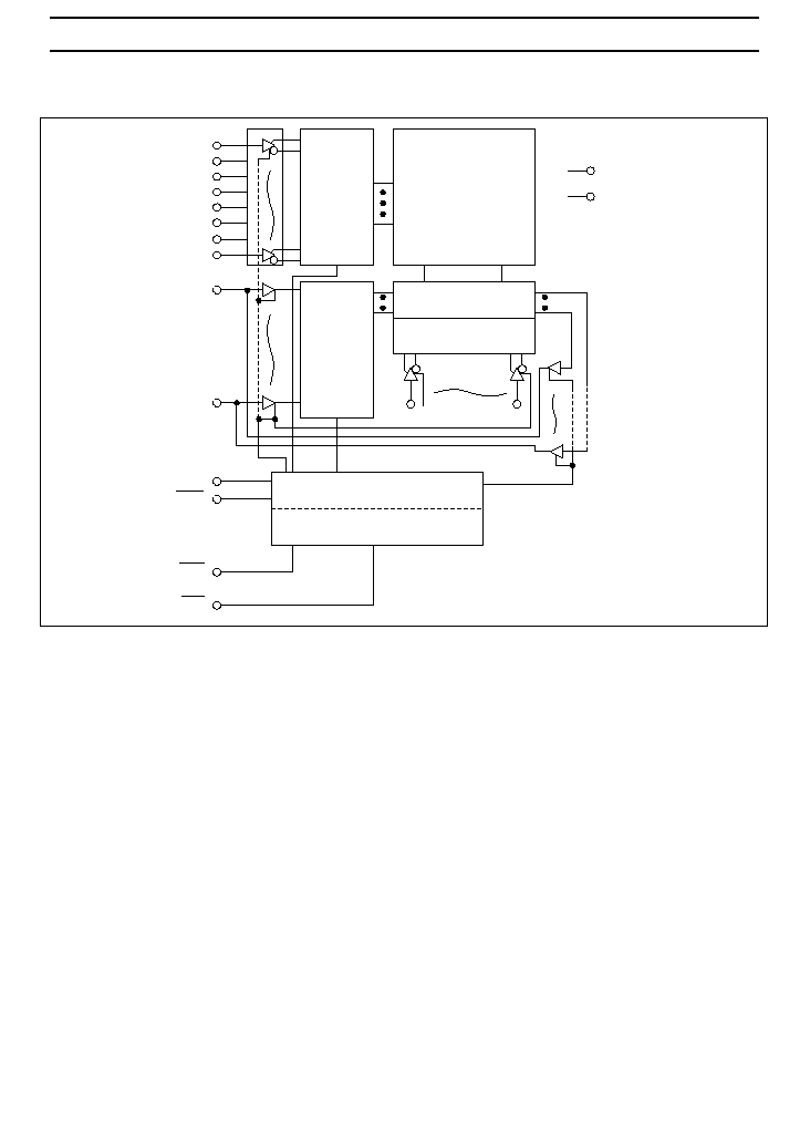
Description
The Hitachi HM9264B is 64k-bit static RAM organized 8-kword
Î
8-bit. It realizes higher performance
and low power consumption by 1.5
Á
m CMOS process technology. The device, packaged in 450 mil
SOP (foot print pitch width), 600 mil plastic DIP, is available for high density mounting.
Features
Ě
High speed
Fast access time: 85/100 ns (max)
Ě
Low power
Standby: 10
Á
W (typ)
Operation: 15 mW (typ) (f = 1 MHz)
Ě
Single 5 V supply
Ě
Completely static memory
No clock or timing strobe required
Ě
Equal access and cycle times
Ě
Common data input and output
Three state output
Ě
Directly TTL compatible
All inputs and outputs
Ě
Battery backup operation capability
Note:
HM9264B series can't be applied for Aerospace, Aircraft, Nucleus Plants, Main Flame
Computers, Medical Life-support System, and Automobile Engine Control and Industrial
machines. (e.g. Communication Hubs, NC, and others.)
Ordering Information
Type No.
Access time
Package
HM9264BLFP-8L
HM9264BLFP-10L
85 ns
100 ns
450-mil, 28-pin plastic SOP(FP-28DA)
HM9264BLP-8L
HM9264BLP-10L
85 ns
100 ns
600-mil, 28-pin plastic DIP (DP-28)

HM9264B Series
Function Table
WE
CS1
CS2
OE
Mode
V
CC
current
I/O pin
Ref. cycle
Î
H
Î
Î
Not selected (power down)
I
SB
, I
SB1
High-Z
--
Î
Î
L
Î
Not selected (power down)
I
SB
, I
SB1
High-Z
--
H
L
H
H
Output disable
I
CC
High-Z
--
H
L
H
L
Read
I
CC
Dout
Read cycle (1)ş(3)
L
L
H
H
Write
I
CC
Din
Write cycle (1)
L
L
H
L
Write
I
CC
Din
Write cycle (2)
Note:
Î
: H or L
Absolute Maximum Ratings
Parameter
Symbol
Value
Unit
Power supply voltage
*1
V
CC
ş0.5 to +7.0
V
Terminal voltage
*1
V
T
ş0.5
*2
to V
CC
+ 0.3
*3
V
Power dissipation
P
T
1.0
W
Operating temperature
Topr
0 to + 70
░
C
Storage temperature
Tstg
ş55 to +125
░
C
Storage temperature under bias
Tbias
ş10 to +85
░
C
Notes: 1. Relative to V
SS
2. V
T
min: ş3.0 V for pulse half-width
50 ns
3. Maximum voltage is 7.0 V
Recommended DC Operating Conditions (Ta = 0 to +70
░
C)
Parameter
Symbol
Min
Typ
Max
Unit
Supply voltage
V
CC
4.5
5.0
5.5
V
V
SS
0
0
0
V
Input high voltage
V
IH
2.2
--
V
CC
+ 0.3
V
Input low voltage
V
IL
ş0.3
*1
--
0.8
V
Note:
1. V
IL
min: ş3.0 V for pulse half-width
50 ns

HM9264B Series
DC Characteristics (Ta = 0 to +70
░
C, V
CC
= 5 V
▒
10%, V
SS
= 0 V)
Parameter
Symbol Min
Typ
*1
Max Unit
Test conditions
Input leakage current
|I
LI
|
--
--
2
Á
A
Vin = V
SS
to V
CC
Output leakage current
|I
LO
|
--
--
2
Á
A
CS1
= V
IH
or CS2 = V
IL
or
OE
= V
IH
or
WE
= V
IL
, V
I/O
= V
SS
to V
CC
Operating power supply
current
I
CCDC
--
7
15
mA
CS1
= V
IL
, CS2 = V
IH
, I
I/O
= 0 mA
others = V
IH
/V
IL
Average operating power
supply current
I
CC1
--
30
45
mA
Min cycle, duty = 100%,
CS1
= V
IL
, CS2 = V
IH
, I
I/O
= 0 mA
others = V
IH
/V
IL
I
CC2
--
3
5
mA
Cycle time = 1
Á
s, duty = 100%, I
I/O
= 0 mA
CS1
0.2 V, CS2
V
CC
ş 0.2 V,
V
IH
V
CC
ş 0.2 V, V
IL
0.2 V
Standby power supply
current
I
SB
--
1
3
mA
CS1
= V
IH
, CS2 = V
IL
I
SB1
--
2
50
Á
A
CS1
V
CC
ş 0.2 V, CS2
V
CC
ş 0.2 V or
0 V
CS2
0.2 V, 0 V
Vin
Output low voltage
V
OL
--
--
0.4
V
I
OL
= 2.1 mA
Output high voltage
V
OH
2.4
--
--
V
I
OH
= ş1.0 mA
Notes: 1. Typical values are at V
CC
= 5.0 V, Ta = +25
░
C and not guaranteed.
Capacitance (Ta = 25
░
C, f = 1.0 MHz)
Parameter
Symbol
Min
Typ
Max
Unit
Test conditions
Input capacitance
*1
Cin
--
--
5
pF
Vin = 0 V
Input/output capacitance
*1
C
I/O
--
--
7
pF
V
I/O
= 0 V
Note:
1. This parameter is sampled and not 100% tested.