HM6264BI Series
64k SRAM (8-kword
×
8-bit)
Wide Temperature Range version
ADE-203-492C (Z)
Rev. 3.0
May. 8, 2000
Description
The Hitachi HM6264BI is 64k-bit static RAM organized 8-kword
×
8-bit. It realizes higher performance and
low power consumption by 1.5
µ
m CMOS process technology. The device, packaged in 450 mil SOP (foot
print pitch width), 600 mil plastic DIP, is available for high density mounting.
Features
·
Single 5 V supply: 5 V
±
10%
·
Access time: 100/120 ns (max)
·
Power dissipation:
Standby: 10
µ
W (typ)
Operation: 15 mW (typ) (f = 1 MHz)
·
Completely static memory
No clock or timing strobe required
·
Equal access and cycle times
·
Common data input and output
Three state output
·
Directly TTL compatible
All inputs and outputs
·
Battery backup operation capability
·
Operating temperature range: 40°C to +85°C
HM6264BI Series
2
Ordering Information
Type No.
Access time
Package
HM6264BLPI-10
HM6264BLPI-12
100 ns
120 ns
600-mil, 28-pin plastic DIP (DP-28)
HM6264BLFPI-10T
HM6264BLFPI-12T
100 ns
120 ns
450-mil, 28-pin plastic SOP(FP-28DA)
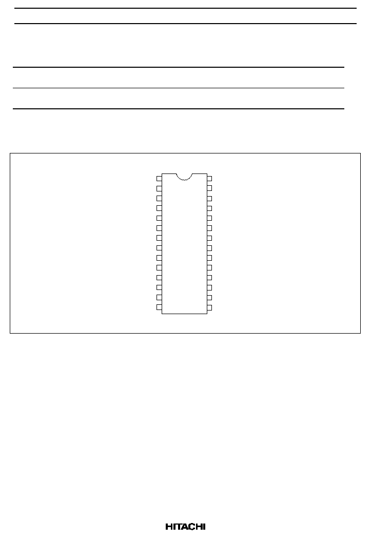
Pin Arrangement
WE
I/O2
27
1
NC
2
A12
3
A7
4
A6
5
A5
6
A4
7
A3
8
A2
9
A1
10
A0
11
I/O1
12
13
14
V
SS
I/O3
V
CC
28
CS2
26
A8
25
A9
24
A11
23
22
A10
21
CS1
20
I/O8
19
I/O7
18
I/O6
17
I/O5
16
I/O4
15
(Top view)
OE
HM6264BLPI/BLFPI Series

HM6264BI Series
4
Function Table
WE
CS1
CS2
OE
Mode
V
CC
current
I/O pin
Ref. cycle
×
H
×
×
Not selected (power down)
I
SB
, I
SB1
High-Z
--
×
×
L
×
Not selected (power down)
I
SB
, I
SB1
High-Z
--
H
L
H
H
Output disable
I
CC
High-Z
--
H
L
H
L
Read
I
CC
Dout
Read cycle (1)(3)
L
L
H
H
Write
I
CC
Din
Write cycle (1)
L
L
H
L
Write
I
CC
Din
Write cycle (2)
Note:
×
: H or L
Absolute Maximum Ratings
Parameter
Symbol
Value
Unit
Power supply voltage*
1
V
CC
0.5 to +7.0
V
Terminal voltage*
1
V
T
0.5*
2
to V
CC
+ 0.3*
3
V
Power dissipation
P
T
1.0
W
Operating temperature
Topr
40 to +85
°
C
Storage temperature
Tstg
55 to +125
°
C
Storage temperature under bias
Tbias
40 to +85
°
C
Notes: 1. Relative to V
SS
2. V
T
min: 3.0 V for pulse half-width
50 ns
3. Maximum voltage is 7.0 V
Recommended DC Operating Conditions (Ta = 40 to +85
°
C)
Parameter
Symbol
Min
Typ
Max
Unit
Supply voltage
V
CC
4.5
5.0
5.5
V
V
SS
0
0
0
V
Input high voltage
V
IH
2.4
--
V
CC
+ 0.3
V
Input low voltage
V
IL
0.3*
1
--
0.6
V
Note:
1. V
IL
min: 3.0 V for pulse half-width
50 ns

HM6264BI Series
5
DC Characteristics (Ta = 40 to +85
°
C, V
CC
= 5 V
±
10%, V
SS
= 0 V)
Parameter
Symbol Min
Typ*
1
Max
Unit Test conditions
Input leakage current
|I
LI
|
--
--
2
µ
A
Vin = V
SS
to V
CC
Output leakage current
|I
LO
|
--
--
2
µ
A
CS1
= V
IH
or CS2 = V
IL
or
OE
= V
IH
or
WE
= V
IL
, V
I/O
= V
SS
to V
CC
Operating power supply
current
I
CCDC
--
7
20
mA
CS1
= V
IL
, CS2 = V
IH
, I
I/O
= 0 mA
others = V
IH
/V
IL
Average operating power
supply current
I
CC1
--
30
50
mA
Min cycle, duty = 100%,
CS1
= V
IL
, CS2 = V
IH
, I
I/O
= 0 mA
others = V
IH
/V
IL
I
CC2
--
3
8
mA
Cycle time = 1
µ
s, duty = 100%, I
I/O
= 0 mA
CS1
0.2 V, CS2
V
CC
0.2 V,
V
IH
V
CC
0.2 V, V
IL
0.2 V
Standby power supply
current
I
SB
--
1
3
mA
CS1
= V
IH
, CS2 = V
IL
I
SB1
*
2
--
2
200
µ
A
CS1
V
CC
0.2 V, CS2
V
CC
0.2 V or
0 V
CS2
0.2 V, 0 V
Vin
Output low voltage
V
OL
--
--
0.4
V
I
OL
= 2.1 mA
Output high voltage
V
OH
2.4
--
--
V
I
OH
= 1.0 mA
Notes: 1. Typical values are at V
CC
= 5.0 V, Ta = +25
°
C and not guaranteed.
2. V
IL
min = 0.3V
Capacitance (Ta = 25
°
C, f = 1.0 MHz)
Parameter
Symbol
Min
Typ
Max
Unit
Test conditions
Input capacitance*
1
Cin
--
--
5
pF
Vin = 0 V
Input/output capacitance*
1
C
I/O
--
--
7
pF
V
I/O
= 0 V
Note:
1. This parameter is sampled and not 100% tested.
