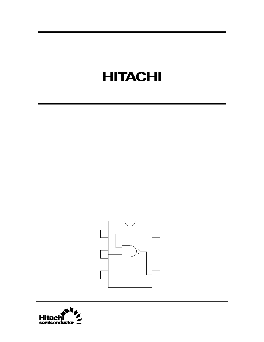
HD74UH00
2-input NAND Gate
ADE-205-014A(Z)
2nd Edition
August 1993
Description
The HD74UH00 is high speed CMOS two input NAND gate using silicon gate CMOS process. With
CMOS low power dissipation, it provides high speed equivalent to LS-TTL series. The internal circuit of
three stages construction with buffer provides wide noise margin and stable output.
Features
·
Encapsulated in very small 5pins package of 2.9
×
1.6
×
1.1 mm, the efficiency to mount on substrate is
significantly improved.
·
The basic gate function is lined up as hitachi uni logic series.
·
Supplied on embos taping for high speed automatic mounting.
·
Electrical characteristics equivalent to the HD74HC00
Supply voltage range: 2 to 6 V
Operating temperature range: 40 to +85°C
·
| I
OH
| = I
OL
= 2 mA (min)
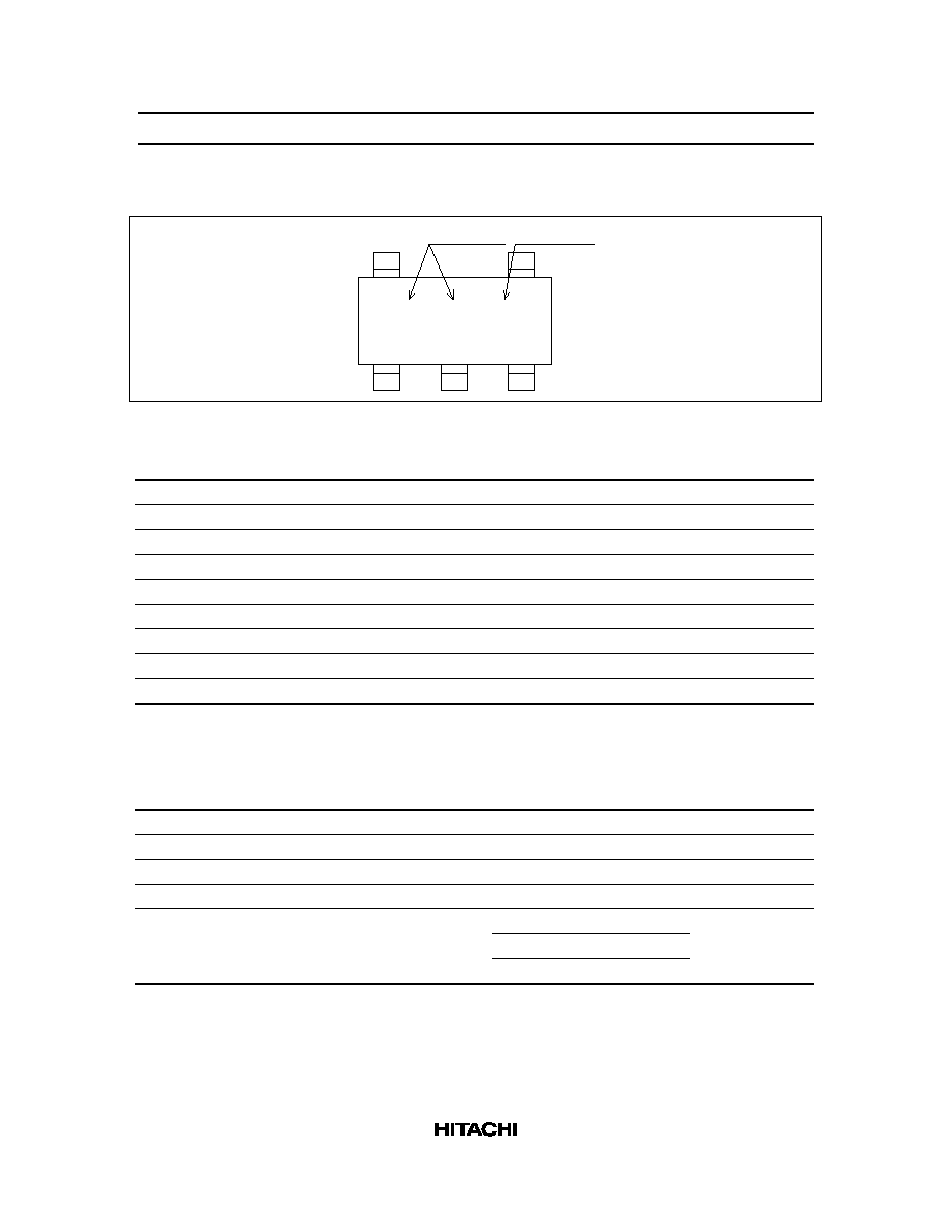
Pin Arrangement
(Top view)
5
4
V
CC
1
2
3
IN B
IN A
GND
OUT X

HD74UH00
4
Ta = 25
°
C
Ta = 40 to
85
°
C
Test Conditions
Item
Symbol
Min
Typ
Max
Min
Max
Unit
V
CC
Output rise/fall time
t
TLH
--
50
125
--
155
ns
2.0
See under figure
t
THL
--
14
25
--
31
4.5
--
12
21
--
26
6.0
Propagation delay time
t
PLH
--
48
100
--
125
ns
2.0
See under figure
t
PHL
--
12
20
--
25
4.5
--
9
17
--
21
6.0
Input capacitance
C
IN
--
5
10
--
10
pF
--
Equivalent capacitance
C
PD
--
10
--
--
--
--
(C
L
= 50 pF, t
r
= t
f
= 6 ns)
Note:
C
PD
is equivalent capacitance inside of the IC calculated from the operating current without load (see
test circuit). The average operating current without load is calculated according to the expression
below.
I
CC
(opr) = C
PD
· V
CC
· f
IN
+ I
CC
Test Circuit
Pulse
generator
50
C
L
Input
Output
V
CC
Note:
Operating current test time, output is open.