HD74BC640A
Octal Bus Transceivers With 3 State Outputs
ADE-205-026 (Z)
Rev.0
June 1993
Description
The HD74BC640A provides high drivability and operation equal to or better than high speed bipolar
standard logic IC by using Bi-CMOS process. The device features low power dissipation that is about 1/5
of high speed bipolar logic IC. When the frequency is 10 MHz. The device has eight bus transceivers with
three state outputs in a 20 pin package. Each device has an active low enable input (
G) and a direction
control input, DiR. When DiR is high, data flows from the A inputs to the B outputs. When DiR is high,
data flows from the B inputs to the A outputs. When enable inputs (
G) is high, disables both A and B ports
by placing then in a high impedance.
Features
·
Input/Output are at high impedance state when power supply is off.
·
Input pins can be open, when not used, owing to built in input pull up circuit.
·
Input is TTL level.
·
Wide operating temperature range
Ta = 40 to +85°C.
Function Table
Control Inputs
G
DIR
Operation
L
L
B
data to A bus
L
H
A
data to B bus
H
X
Isolation
H :
High level
L
:
Low level
X :
Immaterial
HD74BC640A
2
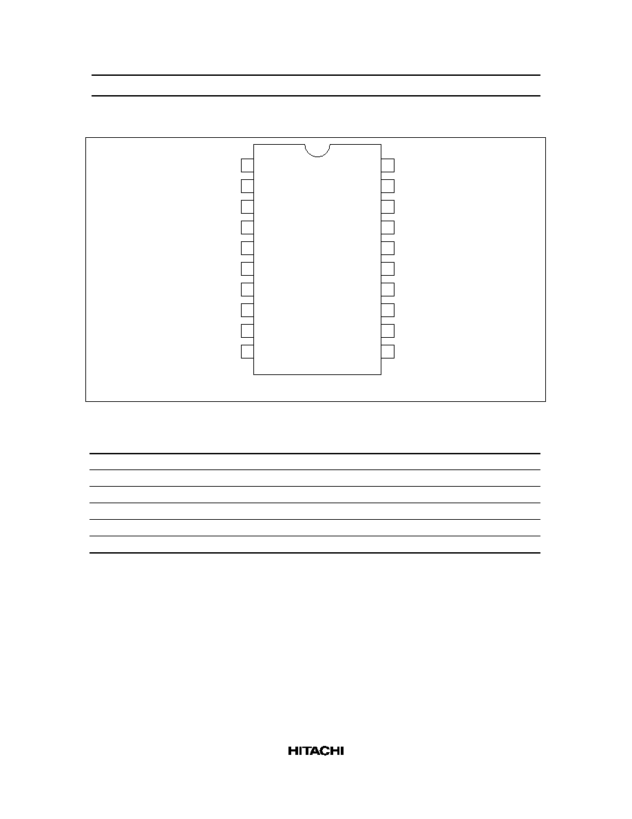
Pin Arrangement
(Top view)
1
2
3
4
5
6
7
8
9
10
11
12
13
14
15
16
17
18
19
20
V
CC
G
B1
B2
B3
B4
B5
B6
B7
B8
DiR
A1
A2
A3
A4
A5
A6
A7
A8
GND
Absolute Maximum Ratings
Item
Symbol
Rating
Unit
Supply voltage
V
CC
0.5 to +7.0
V
Input diode current
I
IK
±
30
mA
Input voltage
V
IN
0.5 to +7.5
V
Output voltage
V
OUT
0.5 to +7.5
V
Off state output voltage
V
OUT(off)
0.5 to +5.5
V
Storage temperature
Tstg
65 to +150
°
C
Note:
1. The absolute maximum ratings are values which must not individually be exceeded, and
furthermore, no two of which may be realized at the same time.
HD74BC640A
3
Recommended Operating Conditions
Item
Symbol
Min
Typ
Max
Unit
Supply voltage
V
CC
4.5
5.0
5.5
V
Input voltage
V
IN
0
--
V
CC
V
Ouput voltage
V
OUT
0
--
V
CC
V
Operating temperature
Topr
40
--
85
°
C
Input rise/fall time*
1
t
r
, t
f
0
--
8
ns/V
Note:
1. This item guarantees maximum limit when one input switches.
Waveform: Refer to test circuit of switching characteristics.
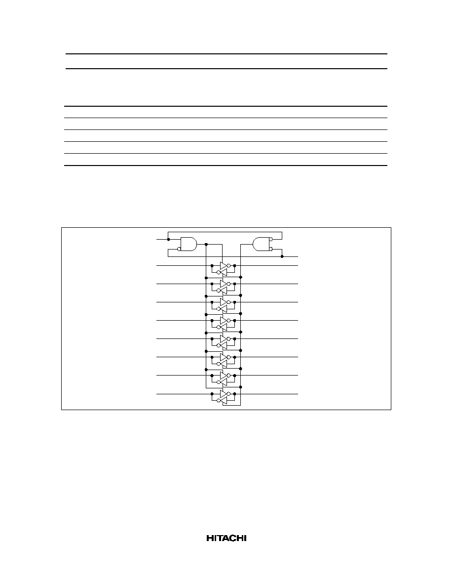
Logic Diagram
B1
B2
B3
B4
B5
B6
B7
A8
A7
A6
A5
A4
A2
A1
DiR
B8
A3
G
HD74BC640A
4
Electrical Characteristics (Ta = 40 to +85°C)
Item
Symbol
V
CC
(V)
Min
Max
Unit
Test Conditions
Input voltage
V
IH
2.0
--
V
V
IL
--
0.8
V
Output voltage
V
OH
4.5
2.4
--
V
I
OH
= 3 mA
4.5
2.0
--
V
I
OH
= 15 mA
V
OL
4.5
--
0.5
V
I
OL
= 48 mA
4.5
--
0.55
V
I
OL
= 64 mA
Input diode voltage
V
IK
4.5
--
1.2
V
I
IN
= 18 mA
Input current
I
I
5.5
--
250
µ
A
V
IN
= 0 V
5.5
--
100
µ
A
An or Bn, V
IN
= 5.5 V
5.5
--
1.0
µ
A
DiR or
G
, V
IN
= 5.5 V
5.5
--
100
µ
A
DiR or
G
, V
IN
= 7 V
Output short circuit current*
1
I
OS
5.5
100
225
mA
V
O
= 0 V, V
IN
= 0 or 5.5 V
Off state output current
I
OZH
5.5
--
100
µ
A
V
O
= 2.7 V
I
OZL
5.5
--
250
µ
A
V
O
= 0.5 V
Supply current
I
CCL
5.5
--
29.5
mA
V
IN
= 0 or 5.5 V
All outputs is "L"
I
CCH
5.5
--
2.5
mA
V
IN
= 0 or 5.5 V
All outputs is "H"
I
CCZ
5.5
--
4.5
mA
V
IN
= 0 or 5.5 V
All outputs is "Z"
I
CCT
*
2
5.5
--
1.5
mA
V
IN
= 3.4 or 0.5 V
Notes: 1. Not more than one output should be shorted at a time and duration of the short circuit should not
exceed one second.
2. When input by the TTL level, it shows I
CC
increase at per one input pin.