HD151015
9 bit Level Shifter/Transceiver With 3 State Outputs
ADE-205-039C (Z)
3rd. Edition
Jun. 1993
Description
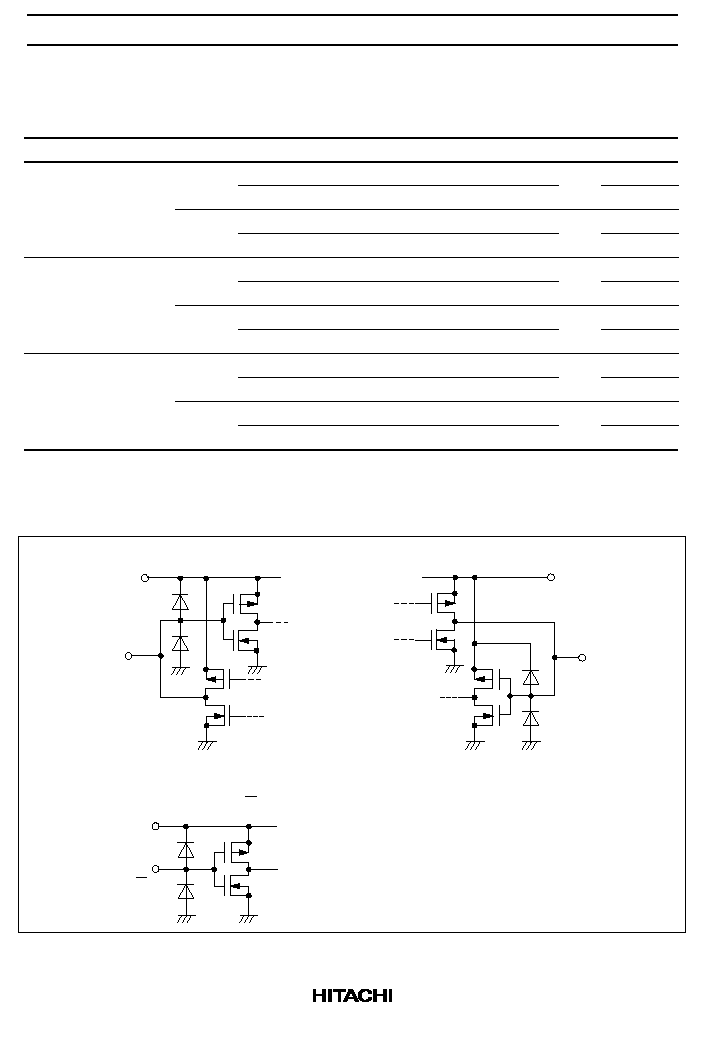
The HD151015 is an IC which consists of 9 bus transceivers (three state output) in a 24 pin package.
Signals are transmitter from A to B when the direction control input (DiR) is at a high level, and from B to
A when DiR is at a low level. When the enable input (
G) is high, A and B are isolated. And this product
has two terminals (V
CCA
, V
CCB
), V
CCA
is connected with control input and A bus side, V
CCB
is connected
with B bus side. V
CCA
and V
CCB
are isolated. Consequently, it is best to change the level in case of two
supply voltage coexist on one board and application of power management.
Features
·
This product function as level shift transceiver that change V
CCA
input level to V
CCB
output level, V
CCB
input level to VCCA output level by providing different supply voltages to V
CCA
and V
CCB
.
·
This product is able to the power management : Turn on and off the supply on V
CCB
side with providing
the supply of V
CCA
.
(Enable input (
G) : High level)
·
Inputs and outputs are CMOS level, and the power dissipation is the same as CMOS standard logic.
·
Wide operating supply voltage range:
V
CCA
= V
CCB
= 2 to 6 V (V
CCB
V
CCA
0.5 V)
·
Wide operating temperature range: Ta = 40 to 85°C
HD151015
3
Absolute Maximum Ratings
Item
Symbol
Rating
Unit
Conditions
Supply Voltage
V
CCA
, V
CCB
0.5 to +7.0
V
Input Diode Current
I
IK
20
mA
V
I
= 0.5
20
mA
V
I
= V
CC
+ 0.5
Input Voltage
V
IN
0.5 to V
CC
+ 0.5
V
Output Diode Current
I
OK
50
mA
V
O
= 0.5
50
mA
V
O
= V
CC
+ 0.5
Output Voltage
V
OUT
0.5 to V
CC
+ 0.5
V
Output Current
I
O
±
50
mA
VCC or Ground Current
I
CC
or I
GND
±
50
mA
per output pin
Storage Temperature
Tstg
65 to + 150
°
C
Note:
1. The absolute maximum ratings are values which must not individually be exceeded, and
furthermore, no two of which may be realized at the same time.
Recommended Operating Conditions
Item
Symbol
Rating
Unit
Conditions
Supply voltage
V
CCA, B
2.0 to 6.0
V
V
CCB
V
CCA
0.5 V
Input voltage
V
IN
0 to V
CC
V
Output voltage
V
OUT
0 to V
CC
V
Operating Temperature
T
A
40 to +85
°
C
Input Rise and Fall Time*
1
t
r
, t
f
8
ns/V
V
CC
@3.0 V (Input DiR,
G
, A)
V
CC
@4.5 V (Input B)
V
CC
@5.5 V (Input B)
Note:
1. The item guarantees maximum limit when one input switches.
Waveform: Refer to test circuit of switching characteristics.
HD151015
4
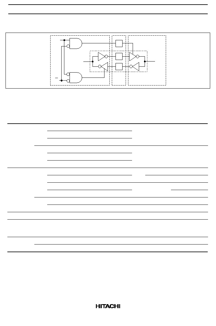
Logick Diagram
G
Transceiver(1/9)
A
B
Level
Change
System
V
System
CCB
V
CCA
System
DIR
Electrical Characteristics
Sym- V
CCA
V
CCB
Ta = 25
°
C
Ta = 40 to
85
°
C
Item
bol
(V) (V)
Min
Typ
Max
Min
Max
Unit
Conditions
Input Voltage V
IH
3.0
3.0
2.1
1.5
--
2.1
--
V
V
OUT
= 0.1 V or V
CC
0.1 V
4.5
4.5
3.15
2.25
--
3.15
--
5.5
5.5
3.85
2.75
--
3.85
--
V
IL
3.0
3.0
--
1.5
0.9
--
0.9
V
V
OUT
= 0.1 V or V
CC
0.1 V
4.5
4.5
--
2.25
1.35
--
1.35
5.5
5.5
--
2.75
1.65
--
1.65
Output
V
OH
2.7
4.5
2.6
2.69
--
2.6
--
V
V
IN
= V
IL
or V
IH
, I
OH
= 50
µ
A A*
1
Voltage
2.7
4.5
4.4
4.49
--
4.4
--
V
IN
= V
IL
or V
IH
, I
OH
= 50
µ
A B
2.7
4.5
2.3
--
--
2.2
--
V
V
IN
=
I
OH
= 4 mA
A
2.7
4.5
3.9
--
--
3.8
--
V
IL
or V
IH
I
OH
= 12 mA B
V
OL
2.7
4.5
--
0.001 0.1
--
0.1
V
V
IN
= V
IL
or V
IH
, I
OL
= 50
µ
A
A.B
2.7
4.5
--
--
0.32
--
0.37
V
V
IN
= V
IL
or V
IH
, I
OL
= 12 mA A.B
Input Current I
IN
3.3
5.5
--
--
±
0.1
--
±
1.0
µ
A
V
IN
= V
CC
or GND
Off State
Output
Current
I
OZ
3.3
5.5
--
--
±
0.5
--
±
5.0
µ
A
V
IN
(
G
) = V
IH
, V
IN
= V
CC
or GND,
V
OUT
= V
CC
or GND
Supply
I
CCA.B
3.3
5.5
--
--
8.0
--
80
µ
A
V
IN
= V
CC
or GND
Current
I
CCA
5.5
0
--
--
8.0
--
80
µ
A
V
IN
= V
CC
or GND, B Input OPEN
Note:
1. A: Output A, B: Output B, A.B: Output A.B