2SK2685
GaAs HEMT
ADE-208-400
1st. Edition
Application
UHF low noise amplifier
Features
ñ
Excellent low noise characteristics.
Fmin = 0.83 dB Typ. (3 V, 10 mA, 2 GHz)
ñ
High associated gain.
Ga = 17 dB Typ. (3 V, 10 mA, 2 GHz)
ñ
High voltage.
V
DS
= 6 or more voltage.
ñ
Small package. (CMPAK-4)
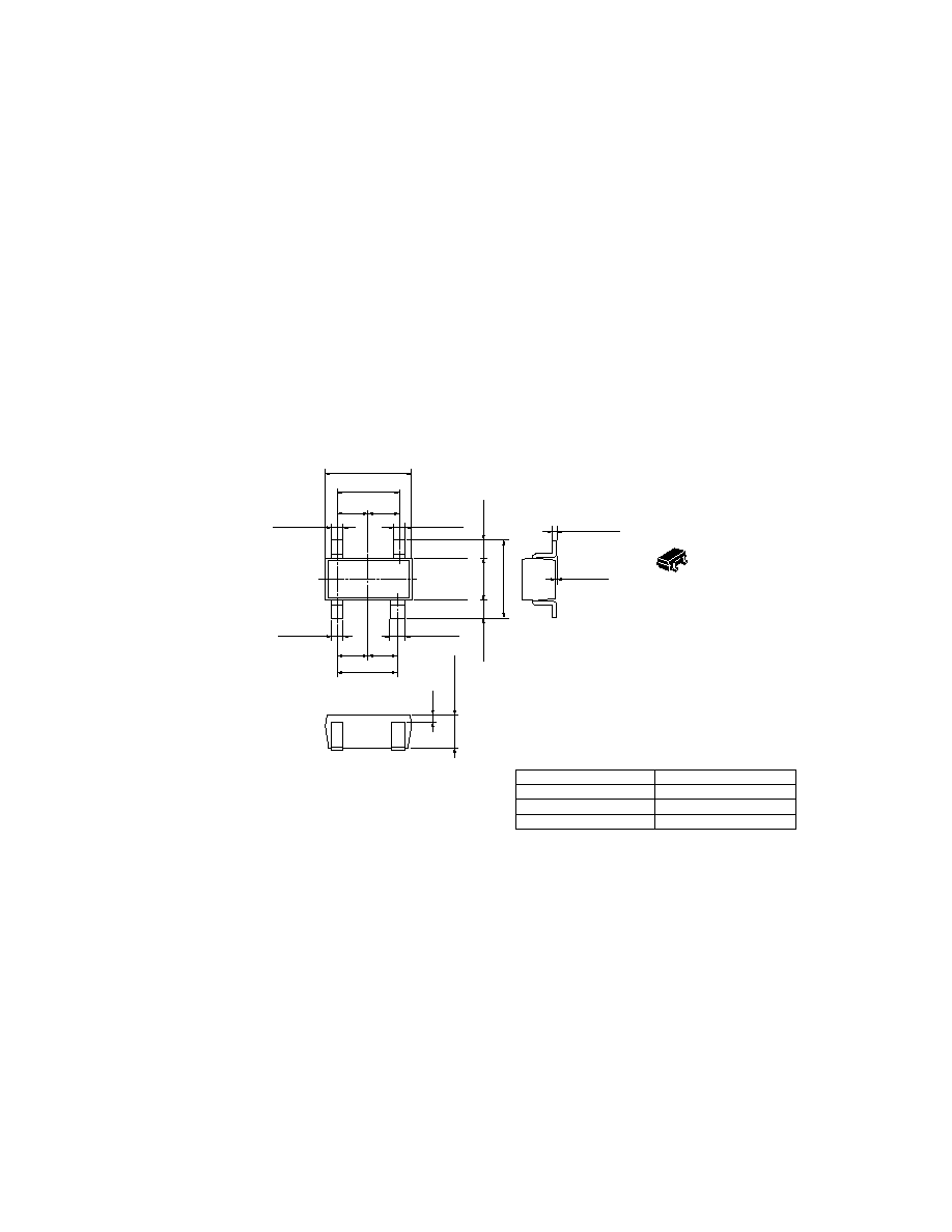
Outline
1. Source
2. Gate
3. Source
4. Drain
CMPAKÙ4
1
4
3
2

2SK2685
2
Absolute Maximum Ratings (Ta = 25¯C)
Item
Symbol
Ratings
Unit
Drain to source voltage
V
DSS
6
V
Gate to source voltage
V
GSO
Ù6
V
Gate to drain voltage
V
GDO
Ù7
V
Drain current
I
D
20
mA
Channel power dissipation
Pch
100
mW
Channel temperature
Tch
125
¯
C
Storage temperature
Tstg
Ù55 to +125
¯
C
Attention: This device is very sensitive to electro static discharge.
It is recommended to adopt appropriate cautions when handling this transistor.
Electrical Characteristics (Ta = 25¯C)
Item
Symbol
Min
Typ
Max
Unit
Test conditions
Gate to source leak current
I
GSS
--
--
Ù20
ç
A
V
GS
= Ù6 V, V
DS
= 0
Gate to source cutoff voltage
V
GS(off)
Ù0.3
--
Ù2.0
V
V
DS
= 3 V, I
D
= 100
ç
A
Drain current
I
DSS
35
50
70
mA
V
DS
= 3 V, V
GS
= 0
(Pulse Test)
Forward transfer admittance
|y
fs
|
40
60
--
mS
V
DS
= 3 V, I
D
= 10 mA,
f = 1 kHz
Associated gain
Ga
--
17.0
--
dB
V
DS
= 3 V, I
D
= 10 mA,
f = 2 GHz
Associated gain
Ga
--
15.2
--
dB
V
DS
= 3 V, I
D
= 3 mA,
f = 2 GHz
Associated gain
Ga
16
21.4
--
dB
V
DS
= 3 V, I
D
= 10 mA,
f = 900 MHz
Associated gain
Ga
--
19.7
--
dB
V
DS
= 3 V, I
D
= 3 mA,
f = 900 MHz
Minimum noise figure
Fmin
--
0.83
--
dB
V
DS
= 3 V, I
D
= 10 mA,
f = 2 GHz
Minimum noise figure
Fmin
--
1.08
--
dB
V
DS
= 3 V, I
D
= 3 mA,
f = 2 GHz
Minimum noise figure
Fmin
--
0.52
1.0
dB
V
DS
= 3 V, I
D
= 10 mA,
f = 900 MHz
Minimum noise figure
Fmin
--
0.74
--
dB
V
DS
= 3 V, I
D
= 3 mA,
f = 900 MHz
Note:
Marking is "ZTÙ".
2SK2685
3
0
200
150
100
50
Ambient Temperature Ta (
¯
C)
Channel Power Dissipation Pch (mW)
200
150
100
50
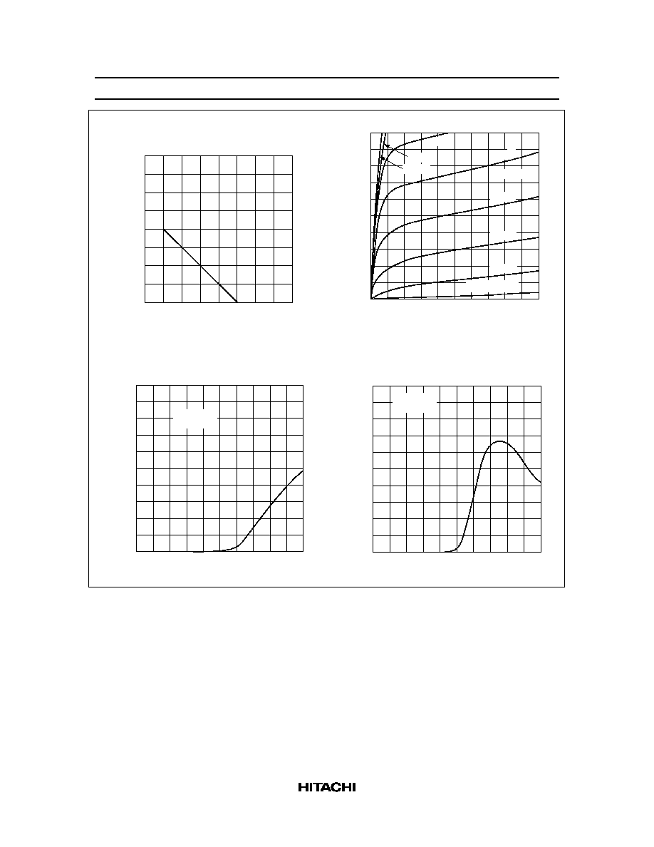
Maximum Channel Power
Dissipation Curve
Typical Output Characteristics
20
16
12
8
4
Drain to Source Voltage V
DS
(V)
0
1
2
3
4
5
Drain Current I
D
(mA)
V
GS
= Ù0.9 V
Ù0.8 V
Ù0.7 V
Ù0.6 V
Ù0.5 V
Ù0.4 V
Pulse Test
Ù0.3 V
Ù0.1 V
Typical Transfer Characteristics
100
80
60
40
20
Ù2.0
Gate to Source Voltage V
GS
(V)
Ù1.6
Ù1.2
Ù0.8
Ù0.4
0
Drain Current I
D
(mA)
V
DS
= 3 V
Pulse Test
Forward Transfer Admittance vs.
Gate to Source Voltage
100
80
60
40
20
0
Gate to Source Voltage V
GS
(V)
Forward Transfer Admittance
yfs
(mS)
Ù2.0
Ù1.6
Ù1.2
Ù0.8
Ù0.4
0
V
DS
= 3 V
Pulse Test
2SK2685
4
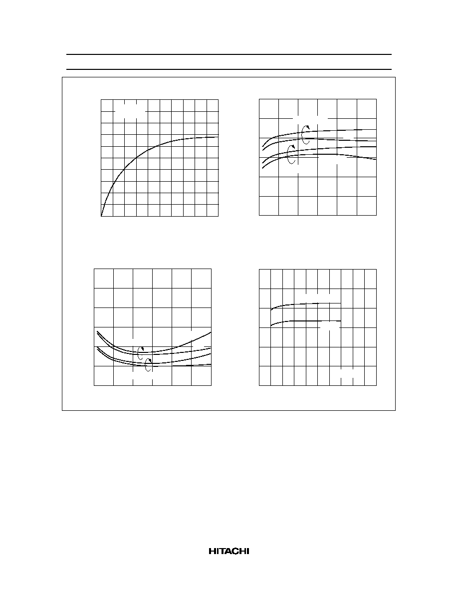
Forward Transfer Admittance vs.
Drain Current
Drain Current I
D
(mA)
Forward Transfer Admittance
yfs
(mS)
4
8
12
16
20
V
DS
= 3 V
Pulse Test
20
40
60
80
100
0
3 V
3 V
1 V
Associated Gain vs. Drain Current
30
20
10
Drain Current I
D
(mA)
0
10
20
30
Associated Gain Ga (dB)
V
DS
= 1 V
f = 2 GHz
f = 900 MHz
Minimum Noise Figure vs. Drain Current
3
2
1
Drain Current I
D
(mA)
0
10
20
30
Minimum Noise Figure Fmin (dB)
3 V
3 V
1 V
V
DS
= 1 V
f = 2 GHz
f = 900 MHz
Associated Gain vs. Drain to Source Voltage
30
20
10
Drain to Source Voltage V
DS
(V)
0
2
4
6
8
10
Associated Gain Ga (dB)
2 GHz
f = 900 MHz
I
D
= 10 mA

2SK2685
5
3.0
2.0
1.0
Drain to Source Voltage V
DS
(V)
0
2
4
6
8
10
Minimum Noise Figure Fmin (dB)
f = 900 MHz
I
D
= 10 mA
2 GHz
Minimum Noise Figure vs.
Drain to Source Voltage
Isolation vs. Drain Current
50
40
30
20
10
Isolation
S21
Ù
S12
(dB)
Drain Current I
D
(mA)
0
10
20
30
3 V
V
DS
= 1 V
f = 900 MHz
Isolation vs. Drain Current
50
40
30
20
10
Isolation
S21
Ù
S12
(dB)
Drain Current I
D
(mA)
0
10
20
30
3 V
V
DS
= 1 V
f = 2 GHz
2SK2685
6
S11 Parameter vs. Frequency
1
Ù1
Ù0.8
0.8
Ù0.6
0.6
Ù0.4
0.4
Ù0.2
0.2
0
1.5
Ù1.5
2
Ù2
Ù3
4
3
Ù4
5
Ù5
10
Ù10
0.2
0.4 0.6 0.8
2
3 4 5
10
1.0
1.5
Condition : I
D
= 10 mA, Zo = 50
200 to 2000 MHz (200 MHz step)
(V
DS
= 1 V)
(V
DS
= 3 V)
S12 Parameter vs. Frequency
90
¯
Ù90
¯
120
¯
Ù120
¯
Ù60
¯
150
¯
Ù150
¯
180
¯
60
¯
30
¯
Ù30
¯
0
¯
Scale : 0.02/div.
Condition : I
D
= 10 mA, Zo = 50
200 to 2000 MHz (200 MHz step)
(V
DS
= 1 V)
(V
DS
= 3 V)
S21 Parameter vs. Frequency
90
¯
Ù90
¯
120
¯
Ù120
¯
Ù60
¯
150
¯
Ù150
¯
180
¯
60
¯
30
¯
Ù30
¯
0
¯
Scale : 2/div.
Condition : I
D
= 10 mA, Zo = 50
200 to 2000 MHz (200 MHz step)
(V
DS
= 1 V)
(V
DS
= 3 V)
S22 Parameter vs. Frequency
1
Ù1
Ù0.8
0.8
Ù0.6
0.6
Ù0.4
0.4
Ù0.2
0.2
0
1.5
Ù1.5
2
Ù2
Ù3
4
3
Ù4
5
Ù5
10
Ù10
0.2
0.4 0.6 0.8
2
3 4 5
10
1.0
1.5
Condition : I
D
= 10 mA, Zo = 50
200 to 2000 MHz (200 MHz step)
(V
DS
= 1 V)
(V
DS
= 3 V)
2SK2685
7
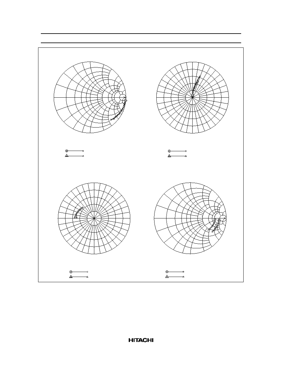
S Parameter (V
DS
= 1 V, I
D
= 10 mA, Z
O
= 50 )
Freq.
S11
S21
S12
S22
(MHz)
MAG.
ANG.
MAG.
ANG.
MAG.
ANG.
MAG.
ANG.
200
0.996
Ù4.8
5.12
175.8
0.00691
89.8
0.688
Ù3.2
400
0.980
Ù9.5
5.13
169.9
0.0143
88.2
0.682
Ù6.5
600
0.977
Ù15.0
5.07
165.4
0.0210
83.3
0.674
Ù10.6
800
0.970
Ù19.9
4.94
161.6
0.0276
81.5
0.668
Ù13.8
1000
0.952
Ù24.4
4.84
156.5
0.0399
79.3
0.658
Ù17.2
1200
0.938
Ù29.2
4.74
152.7
0.0404
76.0
0.648
Ù20.7
1400
0.916
Ù34.0
4.67
147.7
0.0462
74.8
0.636
Ù23.7
1600
0.896
Ù38.2
4.55
144.1
0.0523
73.1
0.622
Ù27.1
1800
0.882
Ù42.9
4.47
140.0
0.0578
72.0
0.611
Ù29.9
2000
0.859
Ù47.1
4.36
135.8
0.0630
70.3
0.597
Ù33.1
S Parameter (V
DS
= 3 V, I
D
= 10 mA, Z
O
= 50
)
Freq.
S11
S21
S12
S22
(MHz)
MAG.
ANG.
MAG.
ANG.
MAG.
ANG.
MAG.
ANG.
200
0.998
Ù4.0
5.13
175.8
0.00581
89.8
0.802
Ù3.2
400
0.988
Ù9.2
5.14
170.1
0.0110
85.5
0.796
Ù6.5
600
0.978
Ù14.5
5.08
165.2
0.0163
83.3
0.790
Ù9.8
800
0.968
Ù19.4
4.95
161.4
0.0216
82.0
0.783
Ù13.3
1000
0.953
Ù24.2
4.85
156.4
0.0363
79.2
0.774
Ù16.4
1200
0.937
Ù28.7
4.75
152.5
0.0312
76.5
0.764
Ù19.4
1400
0.917
Ù33.3
4.68
147.8
0.0358
75.3
0.753
Ù22.5
1600
0.900
Ù37.5
4.57
144.0
0.0401
73.2
0.742
Ù25.4
1800
0.883
Ù41.9
4.49
140.1
0.0442
72.8
0.731
Ù28.1
2000
0.858
Ù46.1
4.37
135.9
0.0477
71.4
0.718
Ù31.1
2.0
Ý
0.2
0.3
2.1
Ý
0.3
0.65 0.6
1.25
Ý
0.2
0.16
0 Ù 0.1
0.9
Ý
0.1
+ 0.1
Ù 0.05
0.4
+ 0.1
Ù 0.05
0.3
+ 0.1
Ù 0.05
+ 0.1
Ù 0.06
0.65 0.65
1.3
Ý
0.2
0.3
+ 0.1
Ù 0.05
0.425
0.425
0.2
Hitachi Code
JEDEC
EIAJ
Weight (reference value)
CMPAK-4(T)
--
Conforms
0.006 g
Unit: mm
1.25
Ý
0.1

Datasheet Title
4
Cautions
1. Hitachi neither warrants nor grants licenses of any rights of Hitachi's or any third party's patent,
copyright, trademark, or other intellectual property rights for information contained in this document.
Hitachi bears no responsibility for problems that may arise with third party's rights, including
intellectual property rights, in connection with use of the information contained in this document.
2. Products and product specifications may be subject to change without notice. Confirm that you have
received the latest product standards or specifications before final design, purchase or use.
3. Hitachi makes every attempt to ensure that its products are of high quality and reliability. However,
contact Hitachi's sales office before using the product in an application that demands especially high
quality and reliability or where its failure or malfunction may directly threaten human life or cause risk
of bodily injury, such as aerospace, aeronautics, nuclear power, combustion control, transportation,
traffic, safety equipment or medical equipment for life support.
4. Design your application so that the product is used within the ranges guaranteed by Hitachi particularly
for maximum rating, operating supply voltage range, heat radiation characteristics, installation
conditions and other characteristics. Hitachi bears no responsibility for failure or damage when used
beyond the guaranteed ranges. Even within the guaranteed ranges, consider normally foreseeable
failure rates or failure modes in semiconductor devices and employ systemic measures such as fail-
safes, so that the equipment incorporating Hitachi product does not cause bodily injury, fire or other
consequential damage due to operation of the Hitachi product.
5. This product is not designed to be radiation resistant.
6. No one is permitted to reproduce or duplicate, in any form, the whole or part of this document without
written approval from Hitachi.
7. Contact Hitachi's sales office for any questions regarding this document or Hitachi semiconductor
products.
1. This product must not be placed in the mouth, as it contains toxic substances that may cause poisoning.
If by chance the product is placed in the mouth, take emergency action such as inducing vomiting, then
consult a physician without delay.
2. Disposal of this product must be handled, separately from other general refuse, by a specialist
processing contractor in the same way as dangerous items.
Datasheet Title
5
Hitachi, Ltd.
Semiconductor & Integrated Circuits.
Nippon Bldg., 2-6-2, Ohte-machi, Chiyoda-ku, Tokyo 100-0004, Japan
Tel: Tokyo (03) 3270-2111 Fax: (03) 3270-5109
Copyright ˋ Hitachi, Ltd., 1998. All rights reserved. Printed in Japan.
Hitachi Asia Pte. Ltd.
16 Collyer Quay #20-00
Hitachi Tower
Singapore 049318
Tel: 535-2100
Fax: 535-1533
URL
NorthAmerica
: http:semiconductor.hitachi.com/
Europe
: http://www.hitachi-eu.com/hel/ecg
Asia (Singapore)
: http://www.has.hitachi.com.sg/grp3/sicd/index.htm
Asia (Taiwan)
: http://www.hitachi.com.tw/E/Product/SICD_Frame.htm
Asia (HongKong)
: http://www.hitachi.com.hk/eng/bo/grp3/index.htm
Japan
: http://www.hitachi.co.jp/Sicd/indx.htm
Hitachi Asia Ltd.
Taipei Branch Office
3F, Hung Kuo Building. No.167,
Tun-Hwa North Road, Taipei (105)
Tel: <886> (2) 2718-3666
Fax: <886> (2) 2718-8180
Hitachi Asia (Hong Kong) Ltd.
Group III (Electronic Components)
7/F., North Tower, World Finance Centre,
Harbour City, Canton Road, Tsim Sha Tsui,
Kowloon, Hong Kong
Tel: <852> (2) 735 9218
Fax: <852> (2) 730 0281
Telex: 40815 HITEC HX
Hitachi Europe Ltd.
Electronic Components Group.
Whitebrook Park
Lower Cookham Road
Maidenhead
Berkshire SL6 8YA, United Kingdom
Tel: <44> (1628) 585000
Fax: <44> (1628) 778322
Hitachi Europe GmbH
Electronic components Group
Dornacher StraÔe 3
D-85622 Feldkirchen, Munich
Germany
Tel: <49> (89) 9 9180-0
Fax: <49> (89) 9 29 30 00
Hitachi Semiconductor
(America) Inc.
179 East Tasman Drive,
San Jose,CA 95134
Tel: <1> (408) 433-1990
Fax: <1>(408) 433-0223
For further information write to: