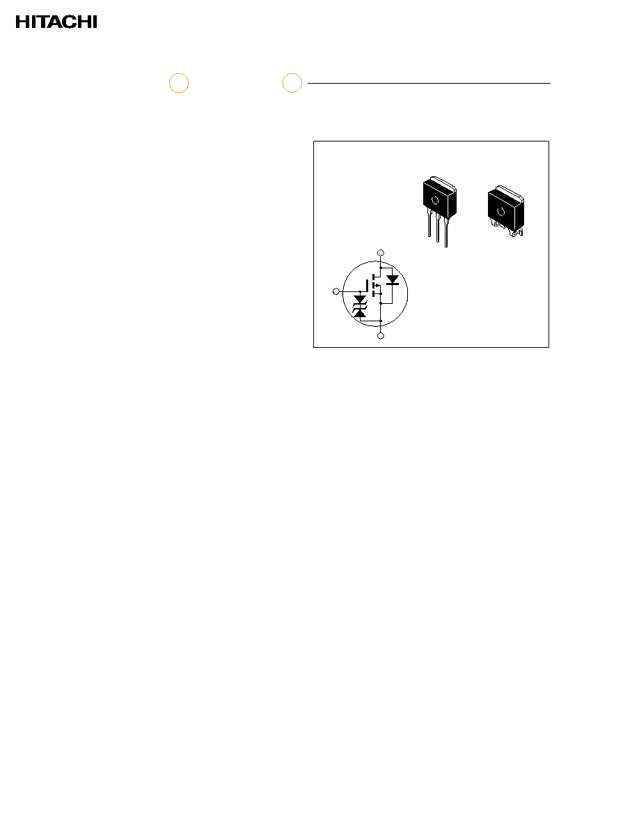
Application
High speed power switching
Features
Ě Low onşresistance
Ě High speed switching
Ě Low drive current
Ě 4 V gate drive device can be driven from
5 V source
Ě Suitable for Switching regulator, DC ş DC
converter
Ě Avalanche Ratings
1
2, 4
3
LDPAK
3
2
1
4
3
2
1
4
1. Gate
2. Drain
3. Source
4. Drain
Table 1 Absolute Maximum Ratings (Ta = 25░C)
Item
Symbol
Ratings
Unit
--------------------------------------------------------------------------------------
Drain to source voltage
V
DSS
ş60
V
--------------------------------------------------------------------------------------
Gate to source voltage
V
GSS
▒20
V
--------------------------------------------------------------------------------------
Drain current
I
D
ş30
A
--------------------------------------------------------------------------------------
Drain peak current
I
D(pulse)
*
ş120
A
--------------------------------------------------------------------------------------
Bodyşdrain diode reverse drain current
I
DR
ş30
A
--------------------------------------------------------------------------------------
Avalanche current
I
AP
***
ş30
A
--------------------------------------------------------------------------------------
Avalanche energy
E
AR
***
77
mJ
--------------------------------------------------------------------------------------
Channel dissipation
Pch**
75
W
--------------------------------------------------------------------------------------
Channel temperature
Tch
150
░C
--------------------------------------------------------------------------------------
Storage temperature
Tstg
ş55 to +150
░C
--------------------------------------------------------------------------------------
*
PW
10 Ás, duty cycle
1 %
**
Value at Tc = 25 ░C
***
Value at Tch = 25 ░C, Rg
50
2SJ280
L
, 2SJ280
S
Silicon P Channel MOS FET

Table 2 Electrical Characteristics (Ta = 25░C)
Item
Symbol
Min
Typ
Max
Unit
Test conditions
--------------------------------------------------------------------------------------
Drain to source breakdown
V
(BR)DSS
ş60
--
--
V
I
D
= ş10 mA, V
GS
= 0
voltage
--------------------------------------------------------------------------------------
Gate to source breakdown
V
(BR)GSS
▒20
--
--
V
I
G
= ▒200 ÁA, V
DS
= 0
voltage
--------------------------------------------------------------------------------------
Gate to source leak current
I
GSS
--
--
▒10
ÁA
V
GS
= ▒16 V, V
DS
= 0
--------------------------------------------------------------------------------------
Zero gate voltage drain current
I
DSS
--
--
ş250
ÁA
V
DS
= ş50 V, V
GS
= 0
--------------------------------------------------------------------------------------
Gate to source cutoff voltage
V
GS(off)
ş1.0
--
ş2.25
V
I
D
= ş1 mA, VDS = ş10 V
--------------------------------------------------------------------------------------
Static drain to source on state
R
DS(on)
--
0.033
0.043
I
D
= ş15 A
resistance
V
GS
= ş10 V *
------------------------------------------------
--
0.045
0.06
I
D
= ş15 A
V
GS
= ş4 V *
--------------------------------------------------------------------------------------
Forward transfer admittance
|y
fs
|
17
25
--
S
I
D
= ş15 A
V
DS
= ş10 V *
--------------------------------------------------------------------------------------
Input capacitance
Ciss
--
3300
--
pF
V
DS
= 10 V
----------------------------------------------------------------
Output capacitance
Coss
--
1500
--
pF
V
GS
= 0
----------------------------------------------------------------
Reverse transfer capacitance
Crss
--
480
--
pF
f = 1 MHz
--------------------------------------------------------------------------------------
Turnşon delay time
t
d(on)
--
30
--
ns
I
D
= ş15 A
----------------------------------------------------------------
Rise time
t
r
--
170
--
ns
V
GS
= ş10 V
----------------------------------------------------------------
Turnşoff delay time
t
d(off)
--
500
--
ns
R
L
= 2
----------------------------------------------------------------
Fall time
t
f
--
390
--
ns
--------------------------------------------------------------------------------------
Bodyşdrain diode forward
V
DF
--
ş1.5
--
V
I
F
= ş30 A, V
GS
= 0
voltage
--------------------------------------------------------------------------------------
Bodyşdrain diode reverse
t
rr
--
200
--
ns
IF = ş30 A, V
GS
= 0,
recovery time
diF / dt = 50 A / Ás
--------------------------------------------------------------------------------------
* Pulse Test
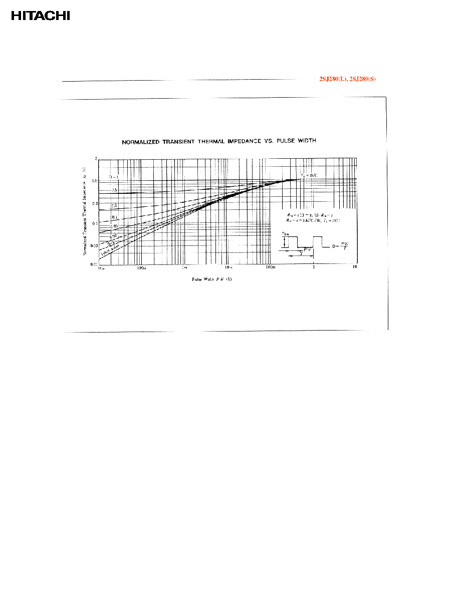
2SJ280 L , 2SJ280 S

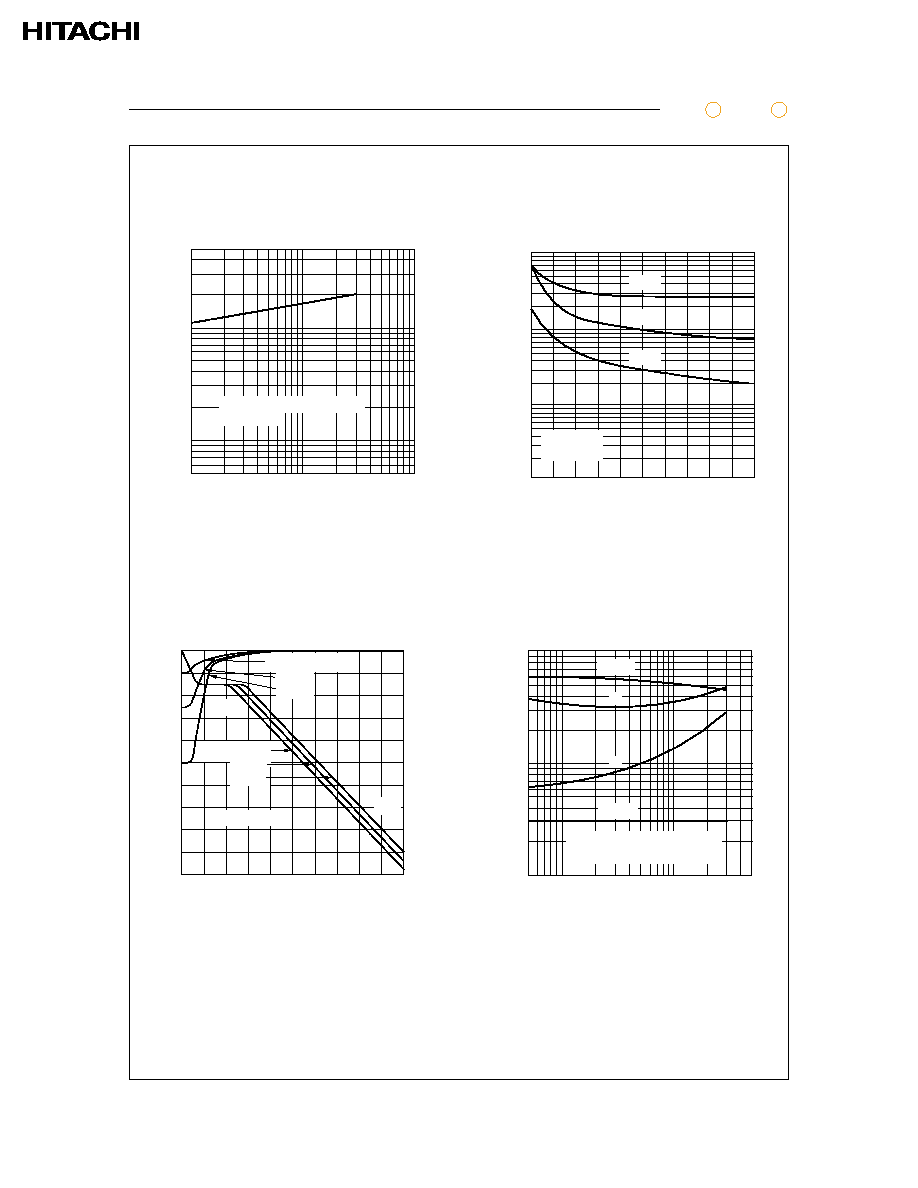
Case Temperature Tc (░C)
Power vs. Temperature Derating
Channel Dissipation Pch (W)
0
25
50
75
50
100
150
Maximum Safe Operation Area
ş500
ş300
ş100
ş30
ş10
ş3
ş1
ş0.5
ş0.1 ş0.3
ş1
ş3
ş10
ş30 ş100
Drain to Source Voltage V (V)
Drain Current I (A)
D
DS
Operation in this area
is limited by R
DS(on)
1 ms
10 s
Á
100 s
Á
PW = 10 ms
DC Operation (Tc = 25░C)
Ta = 25░C
ş2
Typical Output Characteristics
ş50
ş40
ş30
ş20
ş10
0
0
ş4
ş6
ş8
ş10
Drain to Source Voltage V (V)
Drain Current I (A)
D
DS
ş6 V
ş3.5 V
ş4 V
ş2.5 V
V = ş2 V
ş10 V
ş3 V
GS
Typical Transfer Characteristics
ş50
ş40
ş30
ş20
ş10
0
ş1
ş2
ş3
ş4
ş5
Gate to Source Voltage V (V)
Drain Current I (A)
D
GS
Tc = 25░C
75░C
Pulse Test
V = ş10 V
GS
ş25░C
2SJ280 L , 2SJ280 S

Drain-Source Saturation Voltage
vs. Gate-Source Voltage
0
ş2
ş4
ş6
ş8
ş10
ş0.4
ş0.8
ş1.2
ş1.6
ş2.0
Gate to Source Voltage V (V)
Drain to Source Saturation Voltage
V (V)
GS
DS (on)
Pulse Test
ş20 A
ş10 A
I = ş30 A
D
Static Drain-Source on State
Resistance vs. Drain Current
ş2
ş5
ş10 ş20
ş50 ş100 ş200
0.005
0.01
0.02
0.05
0.1
0.2
0.5
Drain Current I (A)
Static Drain-Source on State
Resistance R ( )
DS(on)
D
ş10 V
V = ş4 V
GS
Static Drain-Source on State
Resistance vs. Temperature
Case Temperature T (░C)
C
Static Drain-Source on State
Resistance R ( )
DS(on)
0.1
0.08
0.06
0.04
0.02
ş40
0
40
80
120
160
Pulse test
ş10 V
I = ş30 A
D
V = ş4 V
GS
I = ş30 A
D
ş10 A, ş20 A
ş10 A, ş20 A
0
Forward Transfer Admittance
vs. Drain Current
100
50
20
10
5
2
1
ş0.5
ş1
ş2
ş5
ş20
ş50
ş10
Drain Current I (A)
D
Forward Transfer Admittance
|y | (s)
fs
Tc = 25░C
ş25░C
Pulse Test
V = ş10 V
DS
75░C
2SJ280 L , 2SJ280 S
Body-Drain Diode Reverse
Recovery Time
Reverse Drain Current I (A)
DR
Reverse Recovery Time t (ns)
rr
ş1
ş2
ş5
ş10 ş20
ş50 ş100
5
10
20
50
100
200
500
di/dt = 50 A/ s, V = 0
Ta = 25░C
Á
GS
Typical Capacitance
vs. Drain-Source Voltage
10000
1000
100
10
0
ş10
ş20
ş30
ş40
ş50
Drain to Source Voltage V (V)
DS
Capacitance C (pF)
Ciss
Coss
Crss
V = 0,
f = 1 MHz
GS
Dynamic Input Characteristics
0
ş20
ş40
ş60
ş80
ş100
0
40
80
120
160
200
0
ş4
ş8
ş12
ş16
ş20
Gate Charge Qg (nc)
Drain to Source Voltage V (V)
DS
V = ş10 V
ş25 V
ş50 V
DD
ş25 V
ş50 V
V = ş10 V
DD
V
I = ş30 A
DS
D
Gate to Source Voltage V (V)
GS
V
GS
Switching Characteristics
Drain Current I (A)
D
ş0.5 ş1
ş2
ş5
ş10 ş20
ş50
10
20
50
100
200
500
1000
Switching Time t (ns)
t
t (off)
GS
Á
DD
t (on)
t
<
=
=
:
V = ş10 V, V ş30 V
PW = 2 s, duty 1%
d
d
f
r
2SJ280 L , 2SJ280 S
Reverse Drain Current vs.
Source to Drain Voltage
ş50
ş40
ş30
ş20
ş10
0
0
ş0.4
ş0.8
ş1.2
ş1.6
ş2.0
Source to Drain Voltage V (V)
SD
Reverse Drain Current I (A)
DR
Pulse Test
ş5 V
0, 5V
V = ş10 V
GS
Channel Temperature Tch (░C)
Repetive Avaranche Energy E (mJ)
AR
I = ş30 A
V = ş25 V
duty < 0.1%
Rg 50
DD
AP
>
=
Maxmum Avalanche Energy vs.
Channel Temperature Derating
100
80
60
40
20
0
25
50
75
100
125
150
V
Monitor
DS
I
Monitor
AP
V
DD
Rg
Vin
ş15 V
50
D.U.T
V
DD
0
I
D
I
AP
V
DS
V
(BR)DSS
V
DSS
ş V
DD
V
DSS
E =
AR
2
1 Ě L Ě I Ě
AP
2
L
Avalanche Test Circuit and Waveform
2SJ280 L , 2SJ280 S

Application
High speed power switching
Features
Ě Low onşresistance
Ě High speed switching
Ě Low drive current
Ě 4 V gate drive device can be driven from
5 V source
Ě Suitable for Switching regulator, DC ş DC
converter
Ě Avalanche Ratings
TOş220AB
1
2
3
1. Gate
2. Drain
3. Source
1
2
3
Table 1 Absolute Maximum Ratings (Ta = 25░C)
Item
Symbol
Ratings
Unit
--------------------------------------------------------------------------------------ş
Drain to source voltage
V
DSS
ş60
V
--------------------------------------------------------------------------------------ş
Gate to source voltage
V
GSS
▒20
V
--------------------------------------------------------------------------------------ş
Drain current
I
D
ş15
A
--------------------------------------------------------------------------------------ş
Drain peak current
I
D(pulse)
*
ş60
A
--------------------------------------------------------------------------------------ş
Bodyşdrain diode reverse drain current
I
DR
ş15
A
--------------------------------------------------------------------------------------ş
Avalanche current
I
AP
***
ş15
A
--------------------------------------------------------------------------------------ş
Avalanche energy
E
AR
***
19
mJ
--------------------------------------------------------------------------------------ş
Channel dissipation
Pch**
50
W
--------------------------------------------------------------------------------------ş
Channel temperature
Tch
150
░C
--------------------------------------------------------------------------------------ş
Storage temperature
Tstg
ş55 to +150
░C
--------------------------------------------------------------------------------------ş
*
PW
10 Ás, duty cycle
1 %
**
Value at Tc = 25 ░C
***
Value at Tch = 25 ░C, Rg
50
2SJ290
Silicon P-Channel MOS FET