2SC5246
Silicon NPN Epitaxial
ADE-208-264
1st. Edition
Application
VHF / UHF wide band amplifier
Features
Ě
High gain bandwidth product
f
T
= 12 GHz typ
Ě
High gain, low noise figure
PG = 16.5 dB typ, NF = 1.6 dB typ at f = 900 MHz
Outline
1
2
3
1. Emitter
2. Base
3. Collector
SMPAK

2SC5246
2
Absolute Maximum Ratings (Ta = 25░C)
Item
Symbol
Ratings
Unit
Collector to base voltage
V
CBO
15
V
Collector to emitter voltage
V
CEO
8
V
Emitter to base voltage
V
EBO
1.5
V
Collector current
I
C
20
mA
Collector power dissipation
P
C
80
mW
Junction temperature
Tj
150
░
C
Storage temperature
Tstg
ş55 to +150
░
C
Note:
Marking is "ZCş".
Attention: This device is very sensitive to electro static discharge.
It is recommended to adopt appropriate cautions when handling this transistor.
Electrical Characteristics (Ta = 25░C)
Item
Symbol
Min
Typ
Max
Unit
Test conditions
Collector cutoff current
I
CBO
--
--
10
Á
A
V
CB
= 15 V, I
E
= 0
I
CEO
--
--
1
mA
V
CE
= 8 V, R
BE
=
Emitter cutoff current
I
EBO
--
--
10
Á
A
V
EB
= 1.5 V, I
C
= 0
DC current transfer ratio
h
FE
50
100
160
V
CE
= 5 V, I
C
= 10 mA
Collector output capacitance
Cob
--
0.3
0.8
pF
V
CB
= 5 V, I
E
= 0,
f = 1 MHz
Gain bandwidth product
f
T
9
12
--
GHz
V
CE
= 5 V, I
C
= 5 mA
Power gain
PG
14
16.5
--
dB
V
CE
= 5 V, I
C
= 10 mA,
f = 900 MHz
Noise figure
NF
--
1.6
2.5
dB
V
CE
= 5 V, I
C
= 5 mA,
f = 900 MHz
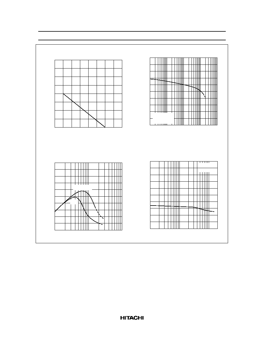
2SC5246
3
160
120
80
40
0
Ambient Temperature Ta (
░
C)
Collector Power Dissipation Pc (mW)
50
100
150
200
Collector Power Dissipation Curve
200
160
120
80
40
Collector Current I (mA)
C
DC Current Transfer Ratio h
FE
0
DC Current Transfer Ratio vs.
Collector Current
V = 5 V
Pulse Test
CE
0.01
0.1
1
10
100
20
16
12
8
4
1
Collector Current I (mA)
C
0
Gain Bandwidth Product vs.
Collector Current
Gain Bandwidth Product f (GHz)
T
2
5
10
20
50
100
V = 5V
CE
1 V
Collector Output Capacitance Cob (pF)
Collector to Base Voltage V (V)
CB
0.1 0.2
0.5
1
2
5
10
20
Collector Output Capacitance vs.
Collector to Base Voltage
1.0
0.2
0.4
I = 0
f = 1 MHz
E
0
0.6
0.8
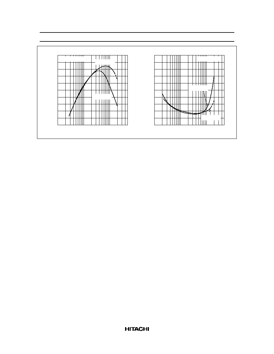
2SC5246
4
20
16
12
8
4
Collector Current I (mA)
50
Power Gain PG (dB)
C
0
Power Gain vs. Collector Current
0.1 0.2
0.5
1
2
5
10 20
f = 900 MHz
V = 5V
CE
V = 1V
CE
10
8
6
4
2
Collector Current I (mA)
50
Noise Figure NF (dB)
C
0
Noise Figure vs. Collector Current
0.1 0.2
0.5
1
2
5
10 20
f = 900 MHz
V = 5V
CE
V = 1V
CE
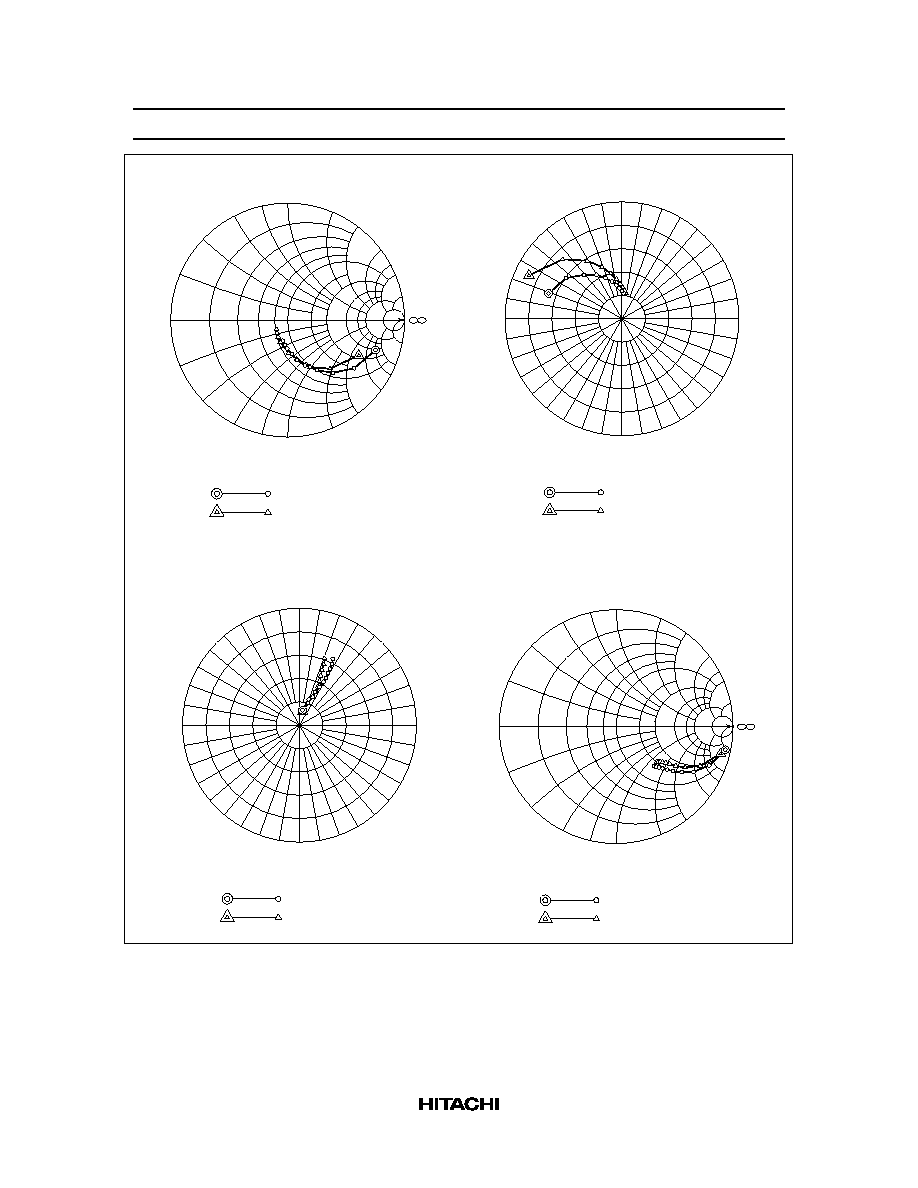
2SC5246
5
Condition: V = 5 V , Zo = 50
200 to 2000 MHz (200 MHz step)
CE
(I = 5 mA)
(I = 10 mA)
C
C
10
5
4
3
2
1.5
1
.8
ş2
ş3
ş4
ş5
ş10
.6
.4
.2
0
ş.2
ş.4
ş.6
ş.8
ş1
ş1.5
.2
.4
.6 .8
2
3 4 5
1.5
10
S11 Parameter vs. Frequency
1.0
Scale: 3 / div.
0
░
30
░
60
░
90
░
120
░
150
░
180
░
ş150
░
ş90
░
ş60
░
ş30
░
ş120
░
Condition: V = 5 V , Zo = 50
200 to 2000 MHz (200 MHz step)
CE
(I = 5 mA)
(I = 10 mA)
C
C
S21 Parameter vs. Frequency
Scale: 0.04 / div.
0
░
30
░
60
░
90
░
120
░
150
░
180
░
ş150
░
ş90
░
ş60
░
ş30
░
ş120
░
Condition: V = 5 V , Zo = 50
200 to 2000 MHz (200 MHz step)
CE
(I = 5 mA)
(I = 10 mA)
C
C
S12 Parameter vs. Frequency
Condition: V = 5 V , Zo = 50
200 to 2000 MHz (200 MHz step)
CE
(I = 5 mA)
(I = 10 mA)
C
C
10
5
4
3
2
1.5
1
.8
ş2
ş3
ş4
ş5
ş10
.6
.4
.2
0
ş.2
ş.4
ş.6
ş.8
ş1
ş1.5
.2
.4
.6 .8
2
3 4 5
1.5
10
S22 Parameter vs. Frequency
1.0