
Subject to local technical requirements and regulations, availability of products included in this promotional material may vary. Please consult with our sales office.
Information furnished by HAMAMATSU is believed to be reliable. However, no responsibility is assumed for possible inaccuracies or omissions.
Specifications are subjected to change without notice. No patent rights are granted to any of the circuits described herein. ˋ 1998 Hamamatsu Photonics K. K.
PRELIMINARY DATA
MAR. 1998
FEATURES
q
High Photocathode Sensitivity
V7090-60 .... GaAs (Cs) Photocathode
V7090-61 .... Blue-enhanced GaAs (Cs) Photocathode
q
Gating Operation ...... 5 ns (Gate Width)
q
High Image Quality
(Multi-boundary deviation and Multi-to-multi deviation
free)
q
No Image Distortion
q
Compact and Lightweight
APPLICATIONS
q
Shutter Camera
q
Low-light-level Imaging
(with image sensors such as CCD, vidicon, etc.)
Microscope, Low-light-level TV, etc.
q
Low-light-level Multichannel Detector
(with linear photodiode array, etc.)
Emission spectroscopy, etc.
Figure 1: Typical Spectral Response
Tll B0074EB
Parameter
V7090U-60-G130
V7090U-61-G130
Unit
Spectral Response
520 to 920
370 to 920
nm
Wavelength of Maximum Response
830
830
nm
Photocathode
Material
GaAs (Cs)
Blue-enhanced GaAs (Cs)
Ù
Minimum Effective Area
18
mm
Material
Borosilicate Glass
Ù
Input Window
Thickness
5.5
mm
Index of Refraction at 589.3nm
1.487
Ù
MCP
1 stage
Ù
Phosphor Screen
Material
P-43
Ù
Minimum Effective Area
18
mm
Output Window Material
Fiber optic plate
Ù
Case Material
Poly Oxy Methylene (POM)
Ù
Lead Wire Cover Material
Teflon
Ù
Weight
80
g
SPECIFICATION
GENERAL
GENERATION
3
3
3
3
3
18mm DIA. PHOTOCATHODE
PROXIMITY FOCUSED
IMAGE INTENSIFIER
V7090 SERIES
WAVELENGTH (nm)
CATHODE RADIANT SENSITIVITY (mA/W)
QUANTUM EFFICIENCY (%)
300
10
-1
10
0
10
1
10
2
10
3
400
500
600
700
800
900
1000
V7090-60
V7090-61
RADIANT SENSITIVITY
QUANTUM EFFICIENCY

PROXIMITY FOCUSED IMAGE INTENSIFIER V7090 SERIES
SELECTION GUIDE BY SUFFIX NUMBER
V7090 A Ù B Ù C D E F
v
v
v
v
v
v
C
Suffix No.
Gate Type
N
Non-Gate
G
Gateable (5ns)
E
Suffix No.
Phosphor Screen
0
P-20
1
P-11
3
P-43
4
P-24
6
P-46
7
P-47
F
Suffix No.
Output Window
0
Fiber Optic Plate
1
Fiber Optic Plate
W/NESA
5
2
Borosilicate Glass
5
With Transparent Conductive
Coating
D
Suffix No.
Stage of MCP
1
1
2
2
3
3
B
Suffix No.
Photocathode
- 60
GaAs (Cs)
- 61
Blue-enhanced
GaAs (Cs)
Radiant
Sensitivity
(Quantum
Efficiency)
Luminous
Gain
b
Radiant
Emittance
Gain
c d
c
The ratio of the phosphor screen radiant emittance in watts per square
meter (W/m
2
) to the irradiance (W/cm
2
) on the photocathode. The
supply voltages are the same as
b
.
d
The value at the wavelength of peak response.
e
The inherent background noise of an image intensifier is normally
specified as the input illuminance (or irradiance) required to produce a
luminous emittance from the phosphor screen, equal to that obtained
when the input illuminance is zero. This indicates the lower limit of
detectable illuminance of an image intensifier.
f
The measure of the ability to detect while and black stripes in an image
formed at the photocathode, in terms of line pairs (Lp) (one black and
one white stripe) per millimeter. This is the value at an MTF (Modulation
Transfer Function) of 5%.
g
1 lm/m
2
=0.0929 ft-L
1 lx =0.0929 ft-c
1 lm/m
2
/lx =1 ft-L/ft-c
RATINGS
Parameter
Value
Maximum Rating
Unit
Photocathode and MCP-In
750 to 800
830
Vdc
1 stage MCP
500 to 900
910
Vdc
Supply Voltage
MCP-In and MCP-Out
2 stage MCP
1000 to 1800
1820
Vdc
3 stage MCP
1500 to 2700
2730
Vdc
MCP-Out and Phosphor Screen
6000
6100
Vdc
Storage
Ù
-55 to +65
¯
C
Temperature
Operating
Ù
-20 to +40
¯
C
Shock
Ù
12
¯
C/min
CHARACTERISTICS
Parameter
V7090-60
V7090-61
Unit
Min.
Typ.
Max.
Min.
Typ.
Max.
Luminous
a
1000
1300
Ù
800
1000
Ù
ç
A/lm
at 450nm
Ù
Ù
Ù
Ù
54 (14.9)
Ù
Photocatohode
at 550nm
Ù
14 (3.2)
Ù
Ù
110 (24.8)
Ù
Sensitivity
at 600nm
Ù
79 (16.3)
Ù
Ù
123 (25.4)
Ù
mA/W (%)
at 700nm
Ù
150 (26.6)
Ù
Ù
143 (25.3)
Ù
at 830nm
Ù
161 (24.0)
Ù
Ù
152 (22.7)
Ù
at 900nm
Ù
11 (1.5)
Ù
Ù
11 (1.5)
Ù
1 stage MCP
2.0
æ
10
4
4.0
æ
10
4
Ù
1.0
æ
10
4
3.0
æ
10
4
Ù
2 stage MCP
4.0
æ
10
6
1.0
æ
10
7
Ù
3.5
æ
10
6
8.0
æ
10
6
Ù
lm/m
2
/lx
g
Light Gain
3 stage MCP
4.0
æ
10
7
1.0
æ
10
8
Ù
3.5
æ
10
7
8.0
æ
10
7
Ù
1 stage MCP
Ù
1.0
æ
10
4
Ù
Ù
9.4
æ
10
3
Ù
2 stage MCP
Ù
2.5
æ
10
6
Ù
Ù
2.3
æ
10
6
Ù
W/m
2
/W/m
2
3 stage MCP
Ù
2.5
æ
10
7
Ù
Ù
2.3
æ
10
7
Ù
EBI
e
Luminous
Ù
2.0
æ
10
-11
5.0
æ
10
-11
Ù
2.0
æ
10
-11
5.0
æ
10
-11
lm/cm
2
Radiant
d
Ù
4.0
æ
10
-14
1.0
æ
10
-13
Ù
4.0
æ
10
-14
1.0
æ
10
-13
W/cm
2
1 stage MCP
36
40
Ù
36
40
Ù
Limiting Resolution
f
2 stage MCP
28
32
Ù
28
32
Ù
Lp/mm
3 stage MCP
25
28
Ù
25
28
Ù
Gate Time (Gate Width)
5
Ù
Ù
5
Ù
Ù
ns
NOTE:
a
The light source is a tungsten filament lamp operated at a distribution
temperature of 2856K. Supply voltage is 800 volts between the
photocathode and all other electrodes (MCP-In, MCP-Out, Phosphor
Screen) connected together as anode.
b
The luminous gain has relation to the screen luminance Lo (cd/m
2
) and
the illuminance Ei (lx) incident on the photocathode, and expressed by:
Luminous Gain =
ñ
The supply voltages are as follows.
Photocathode and MCP-In .............. 800 Vdc
MCP-In and MCP-Out
(1 stage MCP) .... 900 Vdc
(2 stage MCP) .... 1800 Vdc
(3 stage MCP) .... 2700 Vdc
MCP-Out and Phosphor Screen ..... 6000 Vdc
Lo
Ei
A : Potting Form
B : Photocathode
C : Gate Operation
D : Stage of MCP
E : Phosphor screen
F : Output Window
A
Suffix No.
Potting Form
U
See Figure 7
D
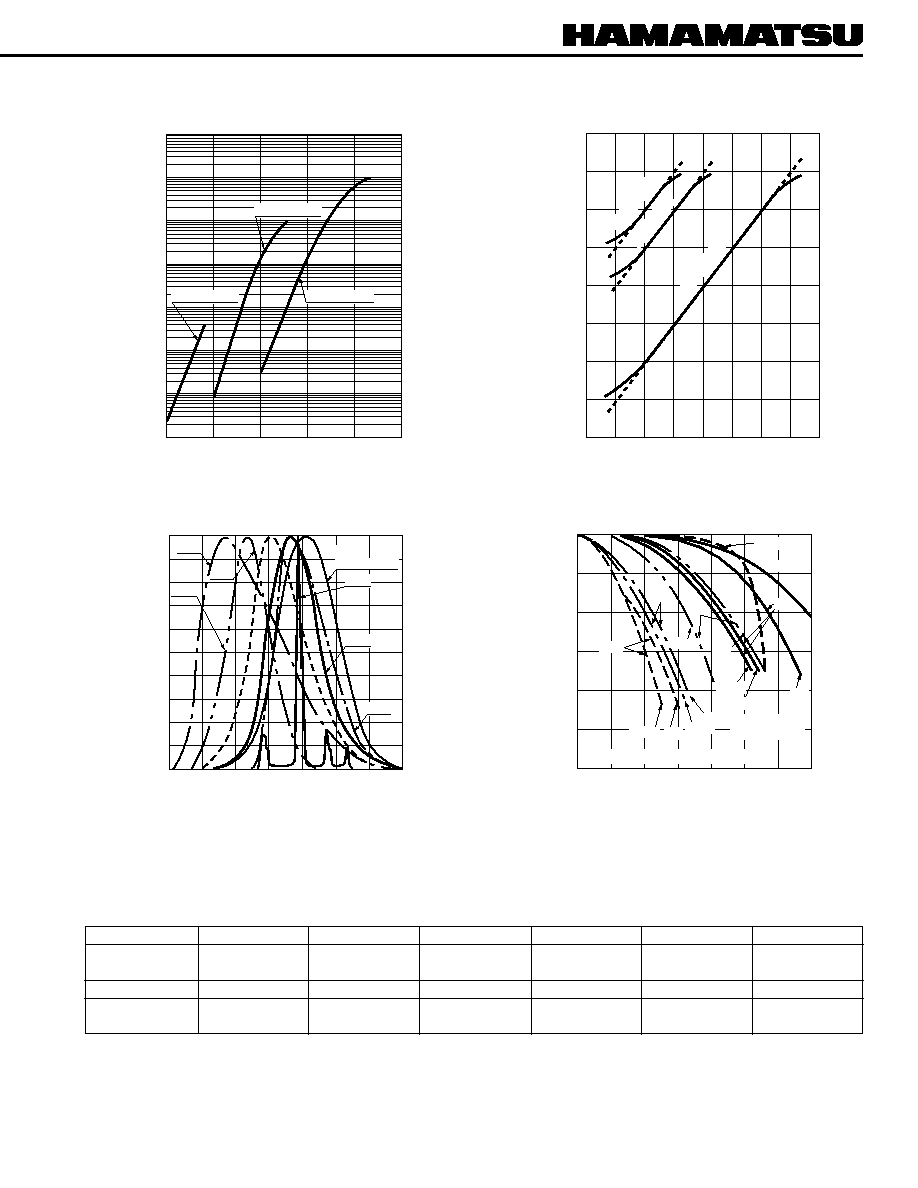
Figure 2: Typical Luminous Gain vs. MCP Voltage
Figure 3: Typical Photocathode Input Illuminance vs.
Phosphor Luminous Emittance
Tll B0076EA
Tll B0075EA
10
Ù9
10
Ù8
10
Ù7
10
Ù6
10
Ù5
10
Ù4
10
Ù3
10
Ù2
10
Ù1
INPUT ILLUMINANCE (lx)
OUTPUT BRIGHTNESS (lm/m
2
/lx)
GAIN=1
æ
10
8
GAIN=1
æ
10
7
GAIN=1
æ
10
4
10
-5
10
-4
10
-3
10
-2
10
-1
10
0
10
1
10
2
10
3
Figure 4: Various Phosphor Screen Spectral Emission
Figure 5: Phosphor Screen Decay Characteristics
Tll B0079EB
Tll B0078EB
Decay Time, Emission Color and Efficiency of Phosphor Screen
Phosphor Screen
P-11
P-20
P-24
P-43
P-46
P-47
Decay Time
30 to 100
ç
s
a
0.01 to 4 ms
a
3 to 40
ç
s
1 ms
0.2 to 100
ç
s
0.1
ç
s
(to 10%)
Emission Color
Blue
Yellowish Green
Green
Yellowish Green
Yellowish Green
Purplish Blue
Relative Power
1
1
0.4
1
0.3
0.3
Efficiency
b
NOTE:
a
Varies with input pulse width.
b
Relative value when P-43 is made as 1. The unit for the power efficiency is expressed W/m
2
.
MCP VOLTAGE (V)
LUMINOUS GAIN (lm/m
2
/lx)
500
1000
1500
2000
2500
3000
10
2
10
3
10
4
10
5
10
6
10
7
10
8
10
9
V7090-61
3 Stage MCP
2 Stage MCP
1 Stage MCP
5
Decay time obtained following to the continuous input light removal.
350
400
450
500
550
600
650
700
WAVELENGTH (nm)
100
80
60
40
20
0
RELATIVE INTENSITY (%)
P-46
P-47
P-11
P-24
P-20
P-43
EYE
RESPONSE
DECAY TIME (s)
RELATIVE INTENSITY (%)
10
-8
10
-4
10
-3
10
-2
10
-1
10
0
10
1
10
2
10
-7
10
-6
10
-5
10
-4
10
-3
10
-2
10
-1
INPUT LIGHT
PULSE WIDTH
100ns
100ns
P-47
P-46
P-24
P-20
P-20DC*
P-43DC*
100ns
100ns
1
ç
s
1ms
1
ç
s
1ms
1ms
SCREEN PEAK CURRENT 8nA/cm
2
HAMAMATSU PHOTONICS K.K., Electron Tube Center
314-5, Shimokanzo, Toyooka-village, Iwata-gun, Shizuoka-ken, 438-0193, Japan, Telephone: (81)539/62-5248, Fax: (81)539/62-2205
U.S.A.: Hamamatsu Corporation: 360 Foothill Road, Bridgewater, N.J. 08807-0910, U.S.A., Telephone: (1)908-231-0960, Fax: (1)908-231-1218
Germany: Hamamatsu Photonics Deutschland GmbH: Arzbergerstr. 10, D-82211 Herrsching am Ammersee, Germany, Telephone: (49)8152-375-0, Fax: (49)8152-2658
France: Hamamatsu Photonics France S.A.R.L.: 8, Rue du Saule Trapu, Parc du Moulin de Massy, 91882 Massy Cedex, France, Telephone: (33)1 69 53 71 00, Fax: (33)1 69 53 71 10
United Kingdom: Hamamatsu Photonics UK Limited: Lough Point, 2 Gladbeck Way, Windmill Hill, Enfield, Middlesex EN2 7JA, United Kingdom, Telephone: (44)181-367-3560, Fax: (44)181-367-6384
North Europe: Hamamatsu Photonics Norden AB: Fðr—gatan 7, S-164-40 Kista, Sweden, Telephone: (46)8-703-29-50, Fax: (46)8-750-58-95
Italy: Hamamatsu Photonics Italia S.R.L.: Via Della Moia, 1/E 20020 Arese, (Milano), Italy, Telephone: (39)2-935 81 733, Fax: (39)2-935 81 741
Tll 1039E02
MAR. 1998. SI
Printed in Japan (500)
Tll B0077EA
0
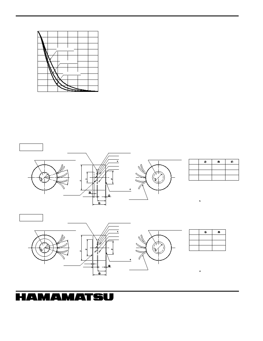
SPATIAL RESOLUTION (Lp/mm)
10
20
30
40
50
60
100
80
60
40
20
90
70
50
30
10
0
MTF (%)
3 Stage MCP
2 Stage MCP
1 Stage MCP
* Gray cable will be connected when the tube has a fiber optic output window with NESA coating, which is expressed as "1" in the suffix-F.
Figure 6: Typical MTF
Figure 7: Dimensional Outline (Unit: mm)
The input window of the type U is depressed from the front surface of its housing.
The input window of the type D is projected from the front surface of its housing.
The input window thickness of both U and D types is 5.5
Ý
0.1mm.
Type. U
Type. D
EFFECTIVE PHOTOCATHODE DIAMETER
18¯
18¯
45.0
+0
Ù0.3
19
GRAY
BLACK
VIOLET
GREEN
RED
21.8
5.5
Ý
0.1
14.2
Ý
0.1
INPUT WINDOW
OUTPUT WINDOW
PHOSPHOR SCREEN
PHOTOCATHODE
LEAD LENGTH
200 MIN.
LEAD
GREEN
VIOLET
BLACK
RED
GRAY
(Teflon Cover)
(PHOTOCATHODE)
(MCP-IN)
(MCP-OUT)
(PHOSPHOR SCREEN)
(NESA/GND)
18 MIN.
EFFECTIVE
PHOSPHOR SCREEN DIAMETER
18 MIN.
INPUT VIEW
OUTPUT VIEW
MCP
23.0
Ý
0.3
2.0
Ý
0.3
0.5
Ý
0.2
1 stage
23.0
Ý
0.3
1.5
Ý
0.3
0.5
Ý
0.2
2 stage
24.0
Ý
0.4
2.0
Ý
0.4
1.5
Ý
0.2
3 stage
Tll A0034EB
Tll A0033EB
EFFECTIVE PHOTOCATHODE DIAMETER
18¯
18¯
45.0
+0
Ù0.3
31.1
BLACK
VIOLET
GREEN
RED
21.8
0.5
Ý
0.2
5.5
Ý
0.1
14.2
Ý
0.1
INPUT WINDOW
LEAD LENGTH
200 MIN.
LEAD
GREEN
VIOLET
BLACK
RED
GRAY
(Teflon Cover)
(PHOTOCATHODE)
(MCP-IN)
(MCP-OUT)
(PHOSPHOR SCREEN)
(NESA/GND)
18 MIN.
EFFECTIVE
PHOSPHOR SCREEN DIAMETER
18 MIN.
INPUT VIEW
OUTPUT VIEW
MCP
21.0
Ý
0.4
0.5
Ý
0.3
1 stage
21.5
Ý
0.4
0.5
Ý
0.3
2 stage
22.0
Ý
0.5
0.5
Ý
0.4
3 stage
PHOSPHOR SCREEN
PHOTOCATHODE
GRAY
OUTPUT WINDOW
PROXIMITY FOCUSED IMAGE INTENSIFIER V7090 SERIES