S8753
Features
Applications
P H O T O D I O D E
Si photodiode
l Dual-element Si photodiode (for visible and infrared range)
l High sensitivity in visible to infrared range
l Small, transparent plastic package: 4 × 4.8 × 1.8
t
mm
l 3-pin SIP lead type (lead length: 4.9 mm)
l Active area: 1.3 × 1.3 mm (× 2 elements)
l Visible and infrared sensors
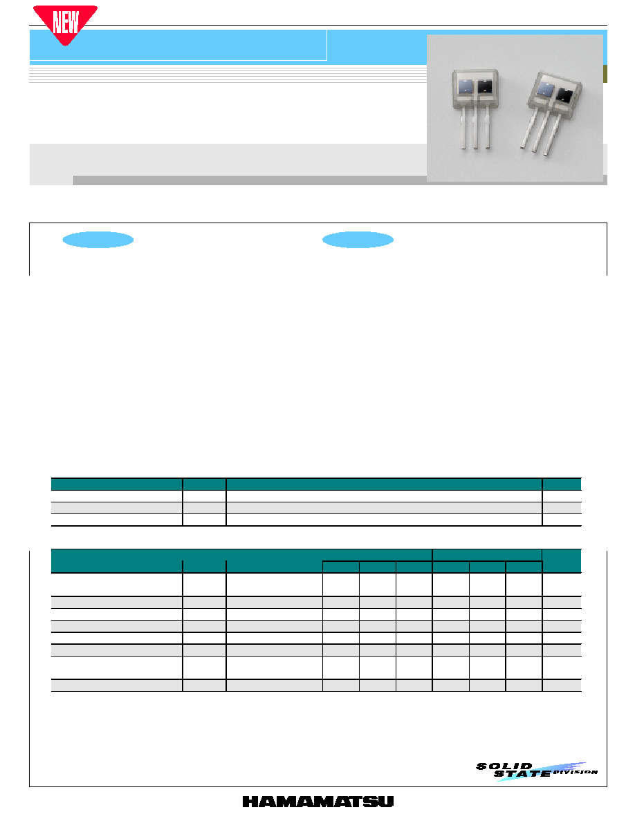
Dual-element photodiode (for visible and infrared range)
S8753 is a visible to infrared sensor using a dual-element photodiode molded into a package. S8753 has two photodiodes with different spectral
response characteristics to deliver high sensitivity over the visible to infrared range. Package material used in S8753 does not cut visible light,
and allows both visible and infrared light to transmit through. The active area size is 1.3 × 1.3 mm (× 2 elements).
PRELIMINARY DATA
Aug. 2002
1
1
I Absolute maximum ratings
Parameter
Symbol
Value
Unit
Reverse voltage
V
R
Max.
10
V
Operating temperature
Topr
-25 to +85
°C
Storage temperature
Tstg
-40 to +100
°C
I Electrical and optical characteristics (Ta=25 °C, per element)
Photodiode a
Photodiode b
Parameter
Symbol
Condition
Min.
Typ.
Max.
Min.
Typ.
Max.
Unit
Spectral response range
l
-
320 to
1000
-
-
800 to
1100
-
nm
Peak sensitivity wavelength
lp
-
720
-
-
960
-
nm
Photo sensitivity
S
l=lp
-
0.4
-
-
0.65
-
A/W
Short circuit current
I
SC
100 lx, 2856 K
-
1.1
-
-
1.3
-
µA
Dark current
I
D
V
R
=1 V, all elements
-
5100
-
5100
pA
Temperature coefficient of I
D
T
CID
-
1.12
-
-
1.12
-
times/°C
Rise time
tr
V
R
=0 V, R
L
=1 kW
10 to 90 %
-
0.2
-
-
0.2
-
µs
Terminal capacitance
Ct
f=1 MHz
-
60
120
-
60
120
pF
Si photodiode
S8753
2
HAMAMATSU PHOTONICS K.K., Solid State Division
1126-1 Ichino-cho, Hamamatsu City, 435-8558 Japan, Telephone: (81) 053-434-3311, Fax: (81) 053-434-5184, http://www.hamamatsu.com
U.S.A.: Hamamatsu Corporation: 360 Foothill Road, P.O.Box 6910, Bridgewater, N.J. 08807-0910, U.S.A., Telephone: (1) 908-231-0960, Fax: (1) 908-231-1218
Germany: Hamamatsu Photonics Deutschland GmbH: Arzbergerstr. 10, D-82211 Herrsching am Ammersee, Germany, Telephone: (49) 08152-3750, Fax: (49) 08152-2658
France: Hamamatsu Photonics France S.A.R.L.: 8, Rue du Saule Trapu, Parc du Moulin de Massy, 91882 Massy Cedex, France, Telephone: 33-(1) 69 53 71 00, Fax: 33-(1) 69 53 71 10
United Kingdom: Hamamatsu Photonics UK Limited: 2 Howard Court, 10 Tewin Road, Welwyn Garden City, Hertfordshire AL7 1BW, United Kingdom, Telephone: (44) 1707-294888, Fax: (44) 1707-325777
North Europe: Hamamatsu Photonics Norden AB: Smidesvägen 12, SE-171 41 Solna, Sweden, Telephone: (46) 8-509-031-00, Fax: (46) 8-509-031-01
Italy: Hamamatsu Photonics Italia S.R.L.: Strada della Moia, 1/E, 20020 Arese, (Milano), Italy, Telephone: (39) 02-935-81-733, Fax: (39) 02-935-81-741
Information furnished by HAMAMATSU is believed to be reliable. However, no responsibility is assumed for possible inaccuracies or omissions.
Specifications are subject to change without notice. No patent rights are granted to any of the circuits described herein. ©2002 Hamamatsu Photonics K.K.
Cat. No. KSPD1057E01
Aug. 2002 DN
2
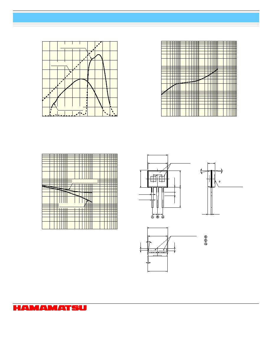
I Dimensional outline (unit: mm)
I Spectral response
KSPDB0211EA
KSPDA0151EA
KSPDB0212EA
WAVELENGTH (nm)
PHOTO SENSITIVITY (A/W)
0
200
400
600
800
1000
1200
0.1
0.2
0.3
0.4
0.5
0.6
0.7
0.8
QE=100 %
PHOTODIODE a
PHOTODIODE b
(Typ. Ta=25 °C)
I Dark current vs. reverse voltage
REVERSE VOLTAGE (V)
DARK CURRENT
100 fA
100 pA
10 pA
1 pA
1
0.1
0.01
10
100
(Typ. Ta=25 °C, all elements)
I Terminal capacitance vs. reverse voltage
KSPDB0213EA
REVERSE VOLTAGE (V)
TERMINAL CAPACITANCE
1 pF
1 nF
100 pF
10 pF
1
0.1
10
100
PHOTODIODE a
PHOTODIODE b
(Typ. Ta=25 °C)
4.7 *
1.8
(2
×
) 10
°
(2
×
) 5
°
4.2 ± 0.2
(INCLUDING BURR)
0.4
0.5
(1.25)
(0.8)
4.9 ± 0.25
4.0 *
5.0 MAX.
(INCLUDING BURR)
(3 ×) 0.5
1.27 1.27
(3 ×) 0.4
0.8
0.25
2.0
DEPTH 0.15 MAX.
PHOTOSENSITIVE
SURFACE
ACTIVE AREA
(1.3 × 1.3)
2.1
(2 ×) 10°
4.7 *
4.8 *
5.0 MAX.
(INCLUDING BURR)
(2 ×) 5°
Photodiode a: visible to infrared range
Photodiode b: visible cut
Tolerance unless otherwise
noted: ±0.1, ±2°
Shaded area indicates burr.
Chip position accuracy with respect
to the package dimensions marked *
X
±0.2, Y±0.2, ±2°
ANODE a
CATHODE COMMON
ANODE b
a
b