
P H O T O D I O D E / P S D
PRELIMINARY DATA
Sep. 2001
S8302
S8302 is a unique light sensor whose active area can be switched to dual-photodiode or PSD by an external signal.
Photodiode/PSD sensor
Dual photodiode or PSD switchable sensor
Features
l
One-dimensional sensor with active area switchable
between dual-photodiode and PSD by external signal
l
Active area: 0.96 × 1.2 mm
Applications
l
Camera auto-focus
l
Optical switch
s Absolute maximum ratings (Ta=25
°
C)
Parameter
Symbol
Value
Unit
Reverse voltage
V
R
Max.10
V
Operating temperature
Topr
-25 to +85
°
C
Storage temperature
Tstg
-40 to +100
°
C
s Electrical and optical characteristics (Ta=25
°
C)
Parameter
Symbol
Condition
Min.
Typ.
Max.
Unit
Spectral response range
-
760 to 1100
-
nm
Peak sensitivity wavelength
p
-
960
-
nm
Photo sensitivity
S
=
p
-
0.55
-
A/W
Vsw *= -4 V (PSD)
100
140
180
Interelectrode resistance
Rie
V
R
=4 V
Vb=0.1 V Vsw *=0 V (dual PD)
1000
-
-
k
Dark current
I
D
V
R
=1 V
-
0.05
1
nA
Temperature coefficient of I
D
-
-
1.15
-
Times/°C
Terminal capacitance
Ct
V
R
=1 V, f=10 kHz
-
10
20
pF
Rise time
tr
V
R
=1 V, R
L
=1 k
-
10
30
µs
Saturation current
Ist
V
R
=1 V, R
L
=1 k
30
-
-
µA
Position detection error
-
V
R
=1 V
Spot light size=
0.1 mm
from center ±75 %
-
±30
±100
µm
* Vsw is the voltage potential at the Vsw terminal versus the cathode.
1
Photodiode/PSD sensor
S8302
s
s
s
s
s
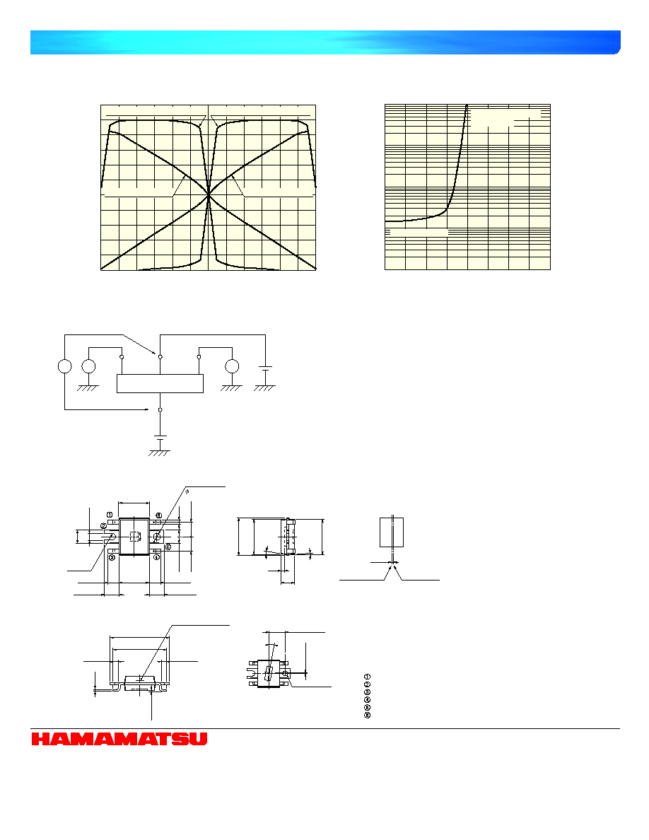
Photocurrent vs. input light position
s
s
s
s
s
Interelectrode resistance vs. V
SW
(Typ. Ta=25 °C)
RELATIVE PHOTOCURRENT (%)
INPUT LIGHT POSITION (mm)
-0.6
0
10
20
30
40
50
60
70
80
90
100
110
0.6
0.5
0.4
0.3
0.2
0.1
0
-0.1
-0.2
-0.3
-0.4
-0.5
DUAL PHOTODIODE CONDITION (I
1
)
PSD CONDITION (I
1
)
PSD CONDITION (I
2
)
DUAL PHOTODIODE CONDITION (I
1
)
(Typ. Ta=25 °C)
Vsw (V)
INTERELECTRODE RESISTANCE (k
)
-4
10
100
1000
10000
100000
-3
-2
-1
0
PSD CONDITION
DUAL PHOTODIODE
CONDITION
KPSDB0076EA
KPSDB0077EA
s
s
s
s
s
Connection example
A
V
SW
ANODE 1
ANODE 2
V
SW
CATHODE
A
PSD
EXTERNAL INPUT
V
R
KPSDA0053EB
s
s
s
s
s
Dimensional outline (unit: mm)
HAMAMATSU PHOTONICS K.K., Solid State Division
1126-1 Ichino-cho, Hamamatsu City, 435-8558 Japan, Telephone: (81) 053-434-3311, Fax: (81) 053-434-5184, http://www.hamamatsu.com
U.S.A.: Hamamatsu Corporation: 360 Foothill Road, P.O.Box 6910, Bridgewater, N.J. 08807-0910, U.S.A., Telephone: (1) 908-231-0960, Fax: (1) 908-231-1218
Germany: Hamamatsu Photonics Deutschland GmbH: Arzbergerstr. 10, D-82211 Herrsching am Ammersee, Germany, Telephone: (49) 08152-3750, Fax: (49) 08152-2658
France: Hamamatsu Photonics France S.A.R.L.: 8, Rue du Saule Trapu, Parc du Moulin de Massy, 91882 Massy Cedex, France, Telephone: 33-(1) 69 53 71 00, Fax: 33-(1) 69 53 71 10
United Kingdom: Hamamatsu Photonics UK Limited: 2 Howard Court, 10 Tewin Road, Welwyn Garden City, Hertfordshire AL7 1BW, United Kingdom, Telephone: (44) 1707-294888, Fax: (44) 1707-325777
North Europe: Hamamatsu Photonics Norden AB: Smidesvägen 12, SE-171 41 Solna, Sweden, Telephone: (46) 8-509-031-00, Fax: (46) 8-509-031-01
Italy: Hamamatsu Photonics Italia S.R.L.: Strada della Moia, 1/E, 20020 Arese, (Milano), Italy, Telephone: (39) 02-935-81-733, Fax: (39) 02-935-81-741
Information furnished by HAMAMATSU is believed to be reliable. However, no responsibility is assumed for possible inaccuracies or omissions.
Specifications are subject to change without notice. No patent rights are granted to any of the circuits described herein. ©2001 Hamamatsu Photonics K.K.
Cat. No. KPSD1018E02
Sep. 2001 DN
KPSDC0070EA
X = 3.0 ± 0.1
Y
± 0.1
± 2°
BASIC HOLE
Chip position accuracy faces
center of standard hole
ANODE 1
CATHODE (COMMON)
ANODE 2
Vsw
CATHODE (COMMON)
CATHODE (COMMON)
4.1 ± 0.2
(INCLUDING BURR)
RESISTANCE LENGTH
1.77
1.5 ± 0.4
4.0
1.905
1.905
1.5 ± 0.4
1.95 ± 0.4
1.95 ± 0.4
R0.4
+0.03
- 0
0.8
+
0.06
-
0
1.77
0.5
0.9
+0.06
- 0
BASIC HOLE
5.0
±
0.2
(INCLUDING BURR)
4.7
4.8
10
°
5
°
1.8
0.5
0.7 ± 0.3
0.7 ± 0.3
0.1 ± 0.1
7.0 ± 0.3
7.9 ± 0.3
PHOTOSENSITIVE
SURFACE
0.25
0.085
CENTER OF
PACKAGE
CENTER OF
ACTIVE AREA
2