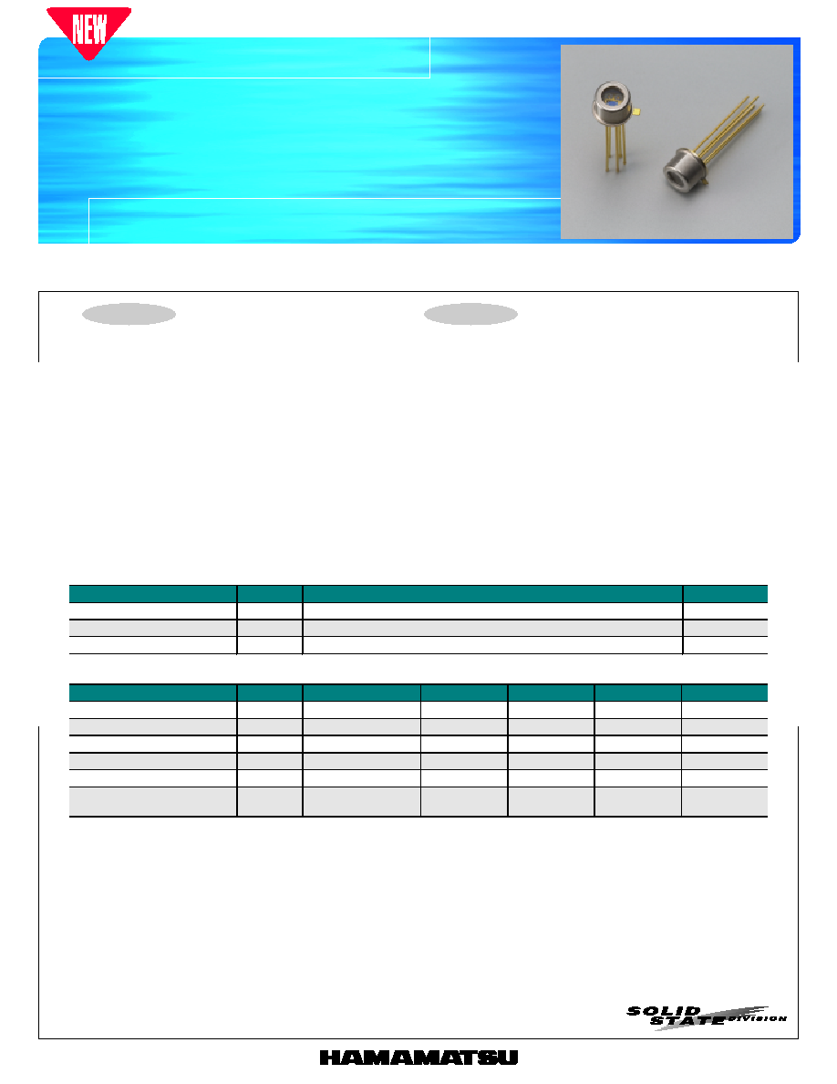
P H O T O D I O D E
PRELIMINARY DATA
Jan. 2001
S8284
S8284 is a high-sensitivity Si PIN photodiode optimized for violet laser detection and especially ideal for optical disc pickups using a violet laser
which has now been put into practical use. S8284 offers 30 % higher sensitivity (at 410 nm) than the conventional type (S1651). S8284 also
features high-speed response at a low bias voltage.
Si PIN photodiode
Quadrant PIN photodiode for violet laser
Features
l
TO-18 package
l
High sensitivity: 0.3 A/W Typ. (
=410 nm)
l
High-speed response: 500 MHz Typ. (V
R
=3 V)
l
Active area: 0.6 × 1.2 mm/4 elements
Applications
l
Violet laser detection
l
Optical disc pickup using violet laser
s
Absolute maximum ratings (Ta=25 °C)
Parameter
Symbol
Value
Unit
Reverse voltage
V
R
Max.
20
V
Operating temperature
Topr
-20 to +100
°
C
Storage temperature
Tstg
-55 to +125
°
C
s
Electrical and optical characteristics (Typ. Ta=25 °C, per 1 element, unless otherwise noted)
Parameter
Symbol
Condition
Min.
Typ.
Max.
Unit
Spectral response range
-
320 to 1000
-
nm
Peak sensitivity wavelength
p
-
760
-
nm
Photo sensitivity
S
=410 nm
0.26
0.30
-
A/W
Dark current
I
D
V
R
=3 V, all elements
-
10
200
pA
Terminal capacitance
Ct
V
R
=3 V, f=1 MHz
-
2
4
pF
Cut-off frequency
fc
V
R
=3 V, R
L
=50
-3 dB
300
500
-
MHz
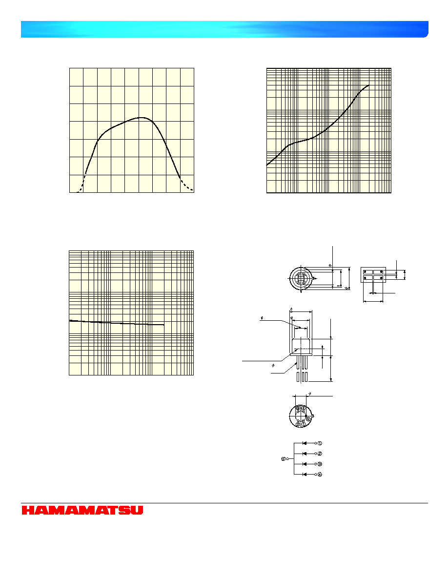
Si PIN photodiode
S8284
a
b
b
c
a
d
c
COMMON TO CASE
d
(14)
(1.6)
4.0 ± 0.2
0.45
LEAD
4.7 ± 0.1
4.7 ± 0.1
3.0 ± 0.1
5.4 ± 0.2
1.2
0.6
0.01
0.01
X
Y
5.4 ± 0.2
2.54 ± 0.2
PHOTOSENSITIVE
SURFACE
WINDOW
3.0 ± 0.1
DETAILS OF
PHOTODIODES
WAVELENGTH (nm)
(Typ. Ta=25 °C)
PHOTO SENSITIVITY
(A/W)
200
0
0.1
0.2
0.7
0.6
0.5
0.4
0.3
400
600
800
1000
s
Spectral response
KPINB0195EA
s
Dimensional outline (unit: mm)
s
Dark current vs. reverse voltage
KPINA0022EB
s
Terminal capacitance vs. reverse voltage
(Typ. Ta=25 °C)
100
10
1
REVERSE VOLTAGE (V)
DARK CURRENT
0.1
0.01
100 fA
1 pA
10 pA
100 pA
KPINB0196EA
(Typ. Ta=25 °C)
100
10
1
REVERSE VOLTAGE (V)
TERMINAL CAPACITANCE
0.1
100 fF
10 pF
1 pF
100 pF
KPINB0197EA
HAMAMATSU PHOTONICS K.K., Solid State Division
1126-1 Ichino-cho, Hamamatsu City, 435-8558 Japan, Telephone: (81) 053-434-3311, Fax: (81) 053-434-5184, http://www.hamamatsu.com
U.S.A.: Hamamatsu Corporation: 360 Foothill Road, P.O.Box 6910, Bridgewater, N.J. 08807-0910, U.S.A., Telephone: (1) 908-231-0960, Fax: (1) 908-231-1218
Germany: Hamamatsu Photonics Deutschland GmbH: Arzbergerstr. 10, D-82211 Herrsching am Ammersee, Germany, Telephone: (49) 08152-3750, Fax: (49) 08152-2658
France: Hamamatsu Photonics France S.A.R.L.: 8, Rue du Saule Trapu, Parc du Moulin de Massy, 91882 Massy Cedex, France, Telephone: 33-(1) 69 53 71 00, Fax: 33-(1) 69 53 71 10
United Kingdom: Hamamatsu Photonics UK Limited: 2 Howard Court, 10 Tewin Road, Welwyn Garden City, Hertfordshire AL7 1BW, United Kingdom, Telephone: (44) 1707-294888, Fax: (44) 1707-325777
North Europe: Hamamatsu Photonics Norden AB: Smidesvägen 12, SE-171 41 Solna, Sweden, Telephone: (46) 8-509-031-00, Fax: (46) 8-509-031-01
Italy: Hamamatsu Photonics Italia S.R.L.: Strada della Moia, 1/E, 20020 Arese, (Milano), Italy, Telephone: (39) 02-935-81-733, Fax: (39) 02-935-81-741
Information furnished by HAMAMATSU is believed to be reliable. However, no responsibility is assumed for possible inaccuracies or omissions.
Specifications are subject to change without notice. No patent rights are granted to any of the circuits described herein. ©2001 Hamamatsu Photonics K.K.
Cat. No. KPIN1055E01
Jan. 2001 DN