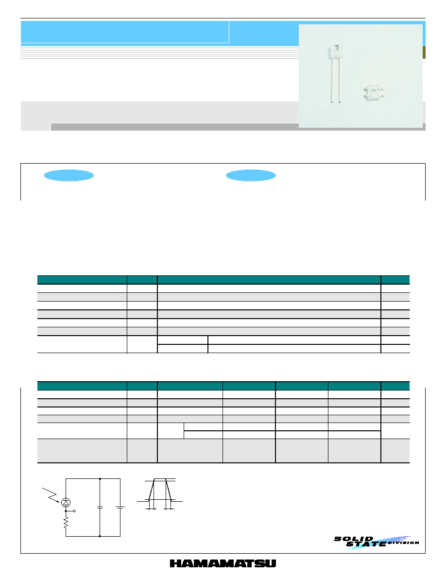
Features
l Clear plastic package
l Operation just as easy as using photodiodes
l Large output current rivaling that of a phototransistor
l Good linearity
Applications
l Energy saving sensors for TV brightness controls, etc.
l Light dimmers for liquid crystal panels
l Various types of light level measurement
P H O T O I C
Photo IC diode
Linear current amplification of photodiode output
S7183, S7184
S7183 and S7184 consist of a photodiode and a signal processing circuit for amplifying the photocurrent generated from the photodiode up to
1300 times. Despite a small active area, these photo ICs provide an output nearly equal to that from photodiodes with a 20 æ 20 mm active area.
Both S7183 and S7184 can be used the same way as a reverse-biased photodiode, and in most cases, they deliver a sufficient output voltage by
just connecting a load resistor.
l=660 nm
LED
PULSE DRIVE
V
O
LOAD RESISTANCE R
L
7.5 V
90 %
2.5 V
10 %
V
O
tr
tf
0.1 çF
KPICC0041EA
s
Absolute maximum ratings (Ta=25 ¯C)
Parameter
Symbol
Value
Unit
Reverse voltage
V
R
-0.5 to 16
V
Photocurrent
I
L
10
mA
Forward current
I
F
10mA
Power dissipation *
1
P
250
mW
Operating temperature
Topr
-30 to +80
¯C
Storage temperature
Tstg
-40 to +85
¯C
S7183
260 ¯C, 3 s, at least 2.5 mm away from package surface
-
Soldering
-
S7184
230 ¯C, 5 s,
*1: Derate power dissipation at a rate of 3.3 mW/¯C above Ta=25 ¯C
s
Electrical and optical characteristics (Ta=25 ¯C)
Parameter
Symbol
Condition
Min.
Typ.
Max.
Unit
Spectral response range
-
300 to 1000
-
nm
Peak sensitivity wavelength
p
-
650
-
nm
Operating reverse voltage
V
R
3
-
12
V
Dark current
I
D
V
R
=5 V
-
0.5
10
nA
S7183, 100 lx
0.75
1.0
1.25
Photocurrent
I
L
V
R
=5 V
2856 K S7184, 1000 lx
1.4
1.8
2.2
mA
Rise/fall time
tr, tf
10 to 90 %, *
2
V
R
=5 V, R
L
=10 k
=660 nm
-
0.6
-
ms
*2: Rise/fall time measurement method

HAMAMATSU PHOTONICS K.K., Solid State Division
1126-1 Ichino-cho, Hamamatsu City, 435-8558 Japan, Telephone: (81) 053-434-3311, Fax: (81) 053-434-5184, http://www.hamamatsu.com
U.S.A.: Hamamatsu Corporation: 360 Foothill Road, P.O.Box 6910, Bridgewater, N.J. 08807-0910, U.S.A., Telephone: (1) 908-231-0960, Fax: (1) 908-231-1218
Germany: Hamamatsu Photonics Deutschland GmbH: Arzbergerstr. 10, D-82211 Herrsching am Ammersee, Germany, Telephone: (49) 08152-3750, Fax: (49) 08152-2658
France: Hamamatsu Photonics France S.A.R.L.: 8, Rue du Saule Trapu, Parc du Moulin de Massy, 91882 Massy Cedex, France, Telephone: 33-(1) 69 53 71 00, Fax: 33-(1) 69 53 71 10
United Kingdom: Hamamatsu Photonics UK Limited: 2 Howard Court, 10 Tewin Road, Welwyn Garden City, Hertfordshire AL7 1BW, United Kingdom, Telephone: (44) 1707-294888, Fax: (44) 1707-325777
North Europe: Hamamatsu Photonics Norden AB: Smidesvðgen 12, SE-171 41 Solna, Sweden, Telephone: (46) 8-509-031-00, Fax: (46) 8-509-031-01
Italy: Hamamatsu Photonics Italia S.R.L.: Strada della Moia, 1/E, 20020 Arese, (Milano), Italy, Telephone: (39) 02-935-81-733, Fax: (39) 02-935-81-741
Information furnished by HAMAMATSU is believed to be reliable. However, no responsibility is assumed for possible inaccuracies or omissions.
Specifications are subject to change without notice. No patent rights are granted to any of the circuits described herein. ˋ2001 Hamamatsu Photonics K.K.
Photo IC diode
S7183, S7184
Cat. No. KPIC1022E01
Mar. 2001 DN
0
200
WAVELENGTH (nm)
RELATIVE SENSITIVITY
400
600
800
1000
1200
(Typ. Ta=25 ¯C, V
R
=5 V)
0.2
0.4
0.6
0.8
1.0
0.1
0.3
0.5
0.7
0.9
s Spectral response
KPICB0036EA
100 fA
-25
AMBIENT TEMPERATURE (¯C)
DARK CURRENT
0
25
50
75
100
(Typ. V
R
=5 V)
1 nA
100 pA
10 pA
1 pA
10 nA
100 nA
1
çA
10
çA
s Dark current vs. ambient
temperature
KPICB0042EA
0.01
100
LOAD RESISTANCE (
)
RISE/F
ALL TIME
(ms)
1 k
10 k
100 k
1 M
(Typ. Ta=25 ¯C, V
R
=5 V,
=560 nm, Vo=2.5 V)
1
0.1
10
100
s Rise/fall time vs. load resistance
KPICB0043EA
CATHODE
DRAWING WITHIN DASHED
LINE SHOWS SCHEMATIC
DIAGRAM OF PHOTO IC DIODE.
ANODE
REVERSE BIAS
POWER SUPPLY
LOAD CAPACITANCE
FOR
LOW-PASS FILTER C
L
R
L
LOAD RESISTANCE
s Operating circuit example
KPICC0018EA
The photodiode must be reverse-biased
so that a positive potential is applied to the
cathode. To eliminate high-frequency
components, we recommend placing a
load capacitance C
L
in parallel with load
resistance R
L
as a low-pass filter.
s Dimensional outlines (unit: mm)
4.3 Ý 0.3
(INCLUDING BURR)
4.15
3.0
2.4
R 0.9
0.45
0.6
10¯
5¯
10¯
5¯
0.45
2.54 Ý 0.5
0.6 Ý 0.3
(0.8)
(1.2)
1.43
4.43
15 MIN.
1.4
Tolerance unless otherwise
noted: Ý0.2, Ý2¯
Shaded area indicates burr.
Values in parentheses are not
guaranteed, but for reference.
1.7
(INCLUDING B
URR)
4.6
+0.6 -0.3
CATHODE
ANODE
(SPECIFIED AT THE LEAD ROOT)
KPICA0017EB
KPICA0018EB
4.1 Ý 0.2
(INCLUDING BURR)
4.0*
2.54
1.5 Ý 0.4
1.5 Ý 0.4
0.6
0.47
5.0
Ý
0.2
(INCLUDING BURR)
4.7*
10¯
4.8
5¯
1.8
0.8
7.0 Ý 0.3
0.25
10¯
5¯
0.7 Ý 0.3
0.7 Ý 0.3
0.1
Ý
0.1
CATHODE
(ANODE)
ANODE
(ANODE)
Tolerance unless otherwise
noted: Ý0.1, Ý2¯
Shaded area indicates burr.
Chip position accuracy with
respect to the package
dimensions marked *
X
Ý0.25, YÝ0.25, GÝ2¯
CENTER OF
ACTIVE AREA
S7183
S7184
Pins and must be
connected to on the
PC board.
Cut-off frequency fc
2
C
L
R
L
1