Features
l Active area: 2.77 × 2.77 mm
l Preamplifier bandwidth: 25 MHz Typ.
Trans-impedance: 30 k
Typ.
l Visible-cut plastic package (5.2 × 9.5 mm)
Applications
l Spatial light transmission
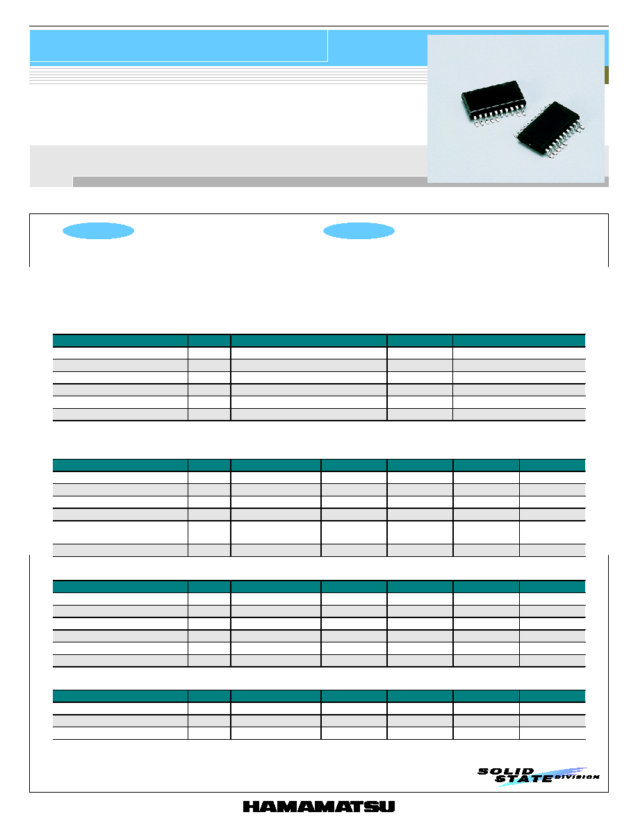
P H O T O D I O D E
Si PIN photodiode with preamp
High-speed photosensor with built-in preamplifier
S5905-02
S5905-02 is a high-speed, high sensitivity photosensor consisting of a large area PIN photodiode and a preamplifier, sealed in a visible-cut plastic
package almost impervious to adverse effects from background disturbance light.
s
Absolute maximum ratings (Ta=25 °C)
Parameter
Symbol
Value
Unit
Note
Reverse voltage
V
R
15
V
Photodiode
Supply voltage
Vcc
-0.5 to +15
V
Preamplifier
Power dissipation *
1
P
1
50
mW
Operating temperature
Topr
-20 to +70
°C
Storage temperature
Tstg
-40 to +100
°C
Soldering
-
230 °C, 5 s
-
*1: Derate power dissipation at a rate of 1.65 mW/°C above Ta=25 °C
s
Electrical and optical characteristics (photodiode, Ta=25 °C)
Parameter
Symbol
Condition
Min.
Typ.
Max.
Unit
Spectral response range
-
760 to 1100
-
nm
Peak sensitivity wavelength
p
-
960
-
nm
Photo sensitivity
S
=900 nm
0.6
0.65
-
A/W
Dark current
I
D
V
R
=12 V
-
0.2
10
nA
Cut-off frequency
fc
V
R
=12 V, R
L
=50
=830 nm, -3 dB
1
0
1
6
-
MHz
Terminal capacitance
Ct
V
R
=12 V, f=1 MHz
-
16
30
pF
s
Electrical characteristics (preamplifier, Ta=25 °C, Vcc=12 V, R
L
=500 , C
L
=20 pF)
Parameter
Symbol
Condition
Min.
Typ.
Max.
Unit
Trans-impedance
R
T
24
30
36
k
Current consumption
Icc
Iin=0, R
L
=
-
-
3
mA
Output voltage at no input
Vo
Iin=0
0.6
0.7
0.85
V
Cut-off frequency
fc
Iin=5 µAp-p
20
25
-
MHz
Maximum input current
Iin
-15
-
-
µA
Equivalent input noise current
in
Iin=0, f=25 MHz
-
1.3
-
pArms/Hz
1/2
s
Operating condition (preamplifier, Ta=25 °C)
Parameter
Symbol
Condition
Min.
Typ.
Max.
Unit
Supply voltage *
2
Vcc
11
12
13
V
Load resistance
R
L
500
-
-
Load capacitance
C
L
-
20
-
pF
*2: A bypass capacitor (0.01 to 0.1 µF ceramic capacitor) is connected between the Vcc and GND leads. The lead length
should be less than 20 mm.
HAMAMATSU PHOTONICS K.K., Solid State Division
1126-1 Ichino-cho, Hamamatsu City, 435-8558 Japan, Telephone: (81) 053-434-3311, Fax: (81) 053-434-5184, http://www.hamamatsu.com
U.S.A.: Hamamatsu Corporation: 360 Foothill Road, P.O.Box 6910, Bridgewater, N.J. 08807-0910, U.S.A., Telephone: (1) 908-231-0960, Fax: (1) 908-231-1218
Germany: Hamamatsu Photonics Deutschland GmbH: Arzbergerstr. 10, D-82211 Herrsching am Ammersee, Germany, Telephone: (49) 08152-3750, Fax: (49) 08152-2658
France: Hamamatsu Photonics France S.A.R.L.: 8, Rue du Saule Trapu, Parc du Moulin de Massy, 91882 Massy Cedex, France, Telephone: 33-(1) 69 53 71 00, Fax: 33-(1) 69 53 71 10
United Kingdom: Hamamatsu Photonics UK Limited: 2 Howard Court, 10 Tewin Road, Welwyn Garden City, Hertfordshire AL7 1BW, United Kingdom, Telephone: (44) 1707-294888, Fax: (44) 1707-325777
North Europe: Hamamatsu Photonics Norden AB: Smidesvägen 12, SE-171 41 Solna, Sweden, Telephone: (46) 8-509-031-00, Fax: (46) 8-509-031-01
Italy: Hamamatsu Photonics Italia S.R.L.: Strada della Moia, 1/E, 20020 Arese, (Milano), Italy, Telephone: (39) 02-935-81-733, Fax: (39) 02-935-81-741
Information furnished by HAMAMATSU is believed to be reliable. However, no responsibility is assumed for possible inaccuracies or omissions.
Specifications are subject to change without notice. No patent rights are granted to any of the circuits described herein. ©2001 Hamamatsu Photonics K.K.
Si PIN photodiode with preamp
S5905-02
Cat. No. KPIC1036E01
Mar. 2001 DN
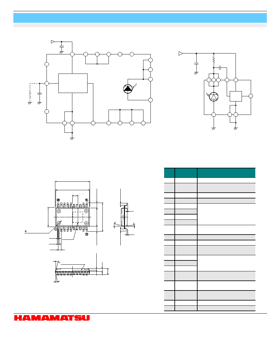
s Block diagram
1
2
19
20
17
15
NC
NC
CATHODE
OUT
R
L
C
L
NC
GND
GND
18
3
IN
5
NC
6
NC
7
NC
8
NC
Vcc
14
NC
13
NC
11
NC
10
NC
16
CATHODE
12
CATHODE
9
ANODE
4
PREAMPLIFIER
0.01 to 0.1
mF
Output voltage Vout = V
O
- R
T
·Iin
Vo: Output voltage at no input
Temperature characteristic -2 mV/°C Typ.
R
T
: Trans-impedance
Temperature characteristic 2500 ppm/°C Typ.
Iin: Input current
KPINC0011EA
s Dimensional outline (unit: mm)
1.5 ± 0.2
0.45
0.89
9.7 ± 0.2
(INCLUDING BURR)
9.5
5.2
8.0 ± 0.3
5.4 ± 0.2
(INCLUDING BURR)
1.4 ± 0.3
1.4 ± 0.3
0.5 ± 0.15
0.8
1.7
0.6 ± 0.3
0.1
15
°
10
°
0.2
0.6 ± 0.3
15°
10°
PHOTOSENSITIVE
SURFACE
ACTIVE
AREA
0.35
1.0 DEPTH 0.15
Tolerance unless otherwise
noted: ±0.1, ±2°
Shaded area indicates burr.
KPINA0054EA
s Application example (for DC light detection)
9 12 16
0.01 TO
0.1
mF
12 V
R (FOR DC LIGHT)
C
(FOR AC LIGHT)
3
17
19
18
2
4
KPINC0059EA
Pin
No.
Name
Function
1NC
No connection
2
GND
Preamplifier ground,
internally connected.
3
IN
Preamplifier input terminal
4
Anode
Photodiode anode
5
NC
6
NC
7
NC
8
NC
No connection.
Internally connected.
9
Cathode Photodiode cathode,
internally connected.
10
NC
No connection
11
NC
No connection
12
Cathode Photodiode cathode,
internally connected.
1
3
NC
14
NC
1
5
NC
No connection.
Internally connected.
16
Cathode Photodiode cathode,
internally connected.
1
7
Vcc
Preamplifier circuit
power supply
18
GND
Preamplifier ground,
internally connected.
19
OUT
Preamplifier output terminal
20
NC
No connection