Features
l
Photo IC for precision printing
Stable output versus laser power or temperature variations
l
S5049-02: For detection of high-speed, high power
laser beams
l
S5049-03: For detection of low power laser beams
Applications
l
Print start timing detection for laser printers, digital copiers,
fax machines, etc.
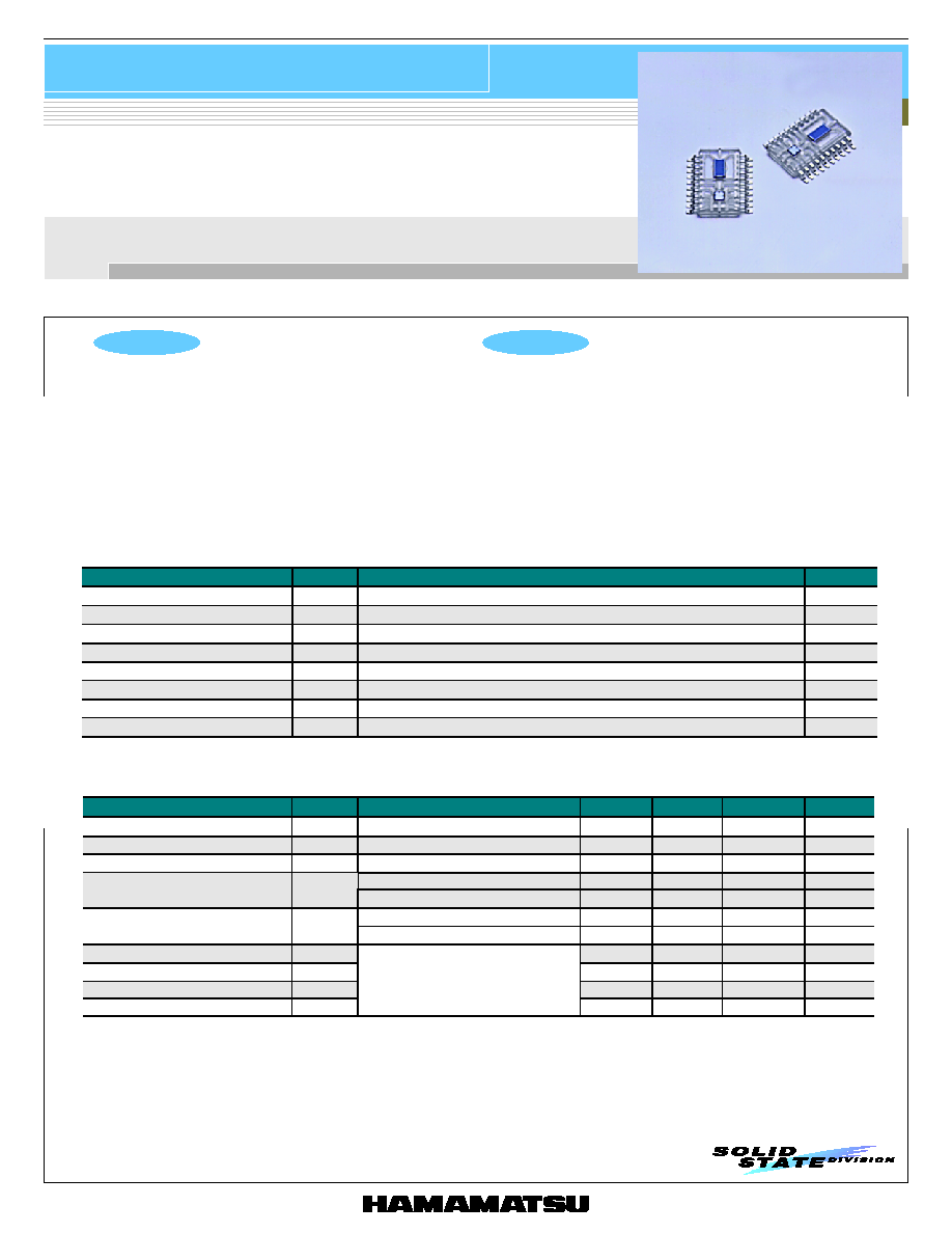
P H O T O I C
Photo IC for laser beam synchronous detection
Photo IC for start timing detection for precise printing
S5049 series
S5049 uses a dual-element PIN photodiode and compares the two photocurrent signals to maintain a highly stable output even when input laser
power or ambient temperature fluctuates. Two types of sensors are available to meet different operating conditions.
s
Absolute maximum ratings (Ta=25 °C, Vcc1=Vcc2=Vcc)
Parameter
Symbol
Value
Unit
Supply voltage
Vcc
-0.5 to +7
V
Power dissipation *
1
P
150
mW
Output voltage
Vo
-0.5 to Vcc
V
Output current
Io
20
mA
Ro
1
, Ro
2
terminal current
I
RO
5
mA
Operating temperature
Topr
-25 to +80
°C
Storage temperature
Tstg
-40 to +85
°C
Soldering
-
230 °C, 5 s
-
*1: Derate power dissipation at a rate of 2 mW/°C above Ta=25 °C.
s
Electrical and optical characteristics (Ta=25
°
C,
=780 nm, Vcc1=Vcc2=Vcc=5 V, Ro1=Ro2=5.1 k
, unless otherwise noted)
Parameter
Symbol
Condition
Min.
Typ
.
Max.
Unit
Supply voltage
Vcc
4.5
5.0
5.5
V
High level output voltage
V
OH
Pin=0
4.9
-
-
V
Low level output voltage
V
OL
Pin=200
µ
W, I
OL
=10 mA
-
0.4
0.6
V
Pin=0, at high level output
-
4.0
6.0
mA
Current consumption
I
CC
Pin=200
µ
W, at low level output
-
6.0
9.0
mA
S5049-02
40
55
70
µ
W
Threshold input power
P
TH
S5049-03
25
35
45
µ
W
H
L propagation delay time variation
t
PHL
-
-
±
10
ns
L
H propagation delay time variation
t
PLH
-
±
50
-
ns
Rise time
tr
-
60
180
ns
Fall time
tf
Pin=200
µ
W at center
Pin=
±
10 % *
2
R
L
=510
, C
L
=15 pF
-
20
100
ns
*2: Beam diameter
(1/e
2
)
=100
µ
m, scan speed=0.5 mm/
µ
s
Not including jitter caused by polygon mirror non-uniformity, etc.
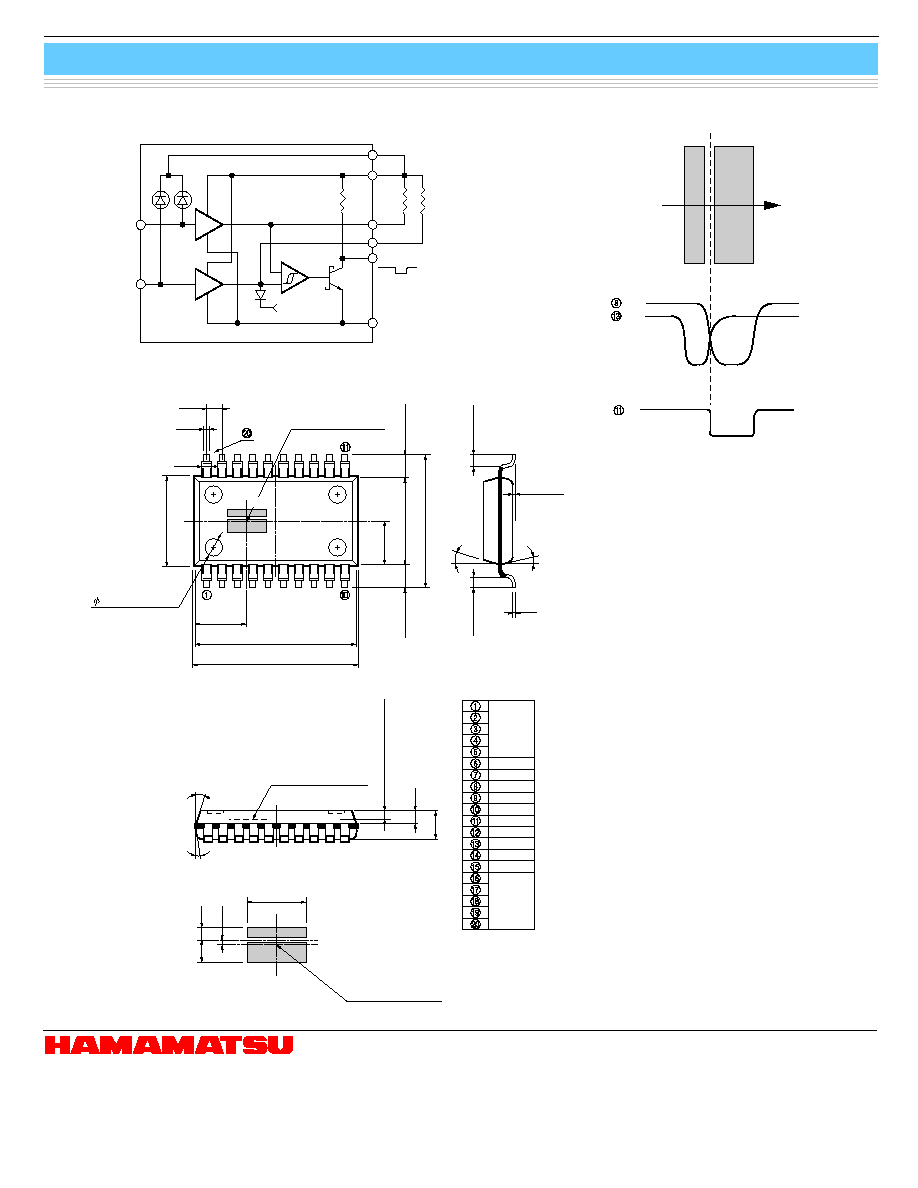
Photo IC for laser beam synchronous detection
S5049 series
HAMAMATSU PHOTONICS K.K., Solid State Division
1126-1 Ichino-cho, Hamamatsu City, 435-8558 Japan, Telephone: (81) 053-434-3311, Fax: (81) 053-434-5184, http://www.hamamatsu.com
U.S.A.: Hamamatsu Corporation: 360 Foothill Road, P.O.Box 6910, Bridgewater, N.J. 08807-0910, U.S.A., Telephone: (1) 908-231-0960, Fax: (1) 908-231-1218
Germany: Hamamatsu Photonics Deutschland GmbH: Arzbergerstr. 10, D-82211 Herrsching am Ammersee, Germany, Telephone: (49) 08152-3750, Fax: (49) 08152-2658
France: Hamamatsu Photonics France S.A.R.L.: 8, Rue du Saule Trapu, Parc du Moulin de Massy, 91882 Massy Cedex, France, Telephone: 33-(1) 69 53 71 00, Fax: 33-(1) 69 53 71 10
United Kingdom: Hamamatsu Photonics UK Limited: 2 Howard Court, 10 Tewin Road, Welwyn Garden City, Hertfordshire AL7 1BW, United Kingdom, Telephone: (44) 1707-294888, Fax: (44) 1707-325777
North Europe: Hamamatsu Photonics Norden AB: Smidesvägen 12, SE-171 41 Solna, Sweden, Telephone: (46) 8-509-031-00, Fax: (46) 8-509-031-01
Italy: Hamamatsu Photonics Italia S.R.L.: Strada della Moia, 1/E, 20020 Arese, (Milano), Italy, Telephone: (39) 02-935-81-733, Fax: (39) 02-935-81-741
Information furnished by HAMAMATSU is believed to be reliable. However, no responsibility is assumed for possible inaccuracies or omissions.
Specifications are subject to change without notice. No patent rights are granted to any of the circuits described herein. ©2001 Hamamatsu Photonics K.K.
Cat. No. KPIC1007E01
Feb. 2001 DN
0.35
0.45
0.89
5.2
(INCLUDING BURR)
5.4 ± 0.2
2.6
±
0.2
8.0 ± 0.3
1.4 ± 0.3
1.4 ± 0.3
3.05 ± 0.2
1.0 DEPTH 0.15
9.5
9.7 ± 0.2
(INCLUDING BURR)
15°
10°
0.1 ± 0.1
0.2
PD1
2.4
0.4
0.7
0.15
PD2
DETAILS OF
PHOTODIODE
PD2
Tolerance unless otherwise
noted: ±0.1, ±2°
Shaded area indicates burr.
CENTER OF CHIP
CENTER OF CHIP
0.5 ± 0.15 (S5049-03)
0.4 ± 0.15 (S5049-02)
0.8
1.7
15°
10°
PHOTOSENSITIVE
SURFACE
V
CC
1
[IN (PD2)]
GND
R
O
2
GND
GND
V
O
GND
R
O
1
V
CC
2
[IN (PD1)]
V
CC
1
Tolerance unless otherwise noted: ±0.03
0.6 ± 0.3
0.6 ± 0.3
PD1
ACTIVE AREA
PD1
PD2
R
O
2
R
O
1
V
O
KPICC0007EA
s
Equivalent circuit
s
Dimensional outline (unit: mm)
10 k
Vref
GND
V
O
R
O
2
EXTERNAL
GAIN
RESISTANCE
V
CC
2
V
CC
1
PD1 PD2
RELAY
TERMINAL
IN (PD2)
RELAY
TERMINAL
IN (PD1)
R
O
1
KPICC0008EB
KPICA0007EB
s
Output waveforms of terminals 8, 11 and 13