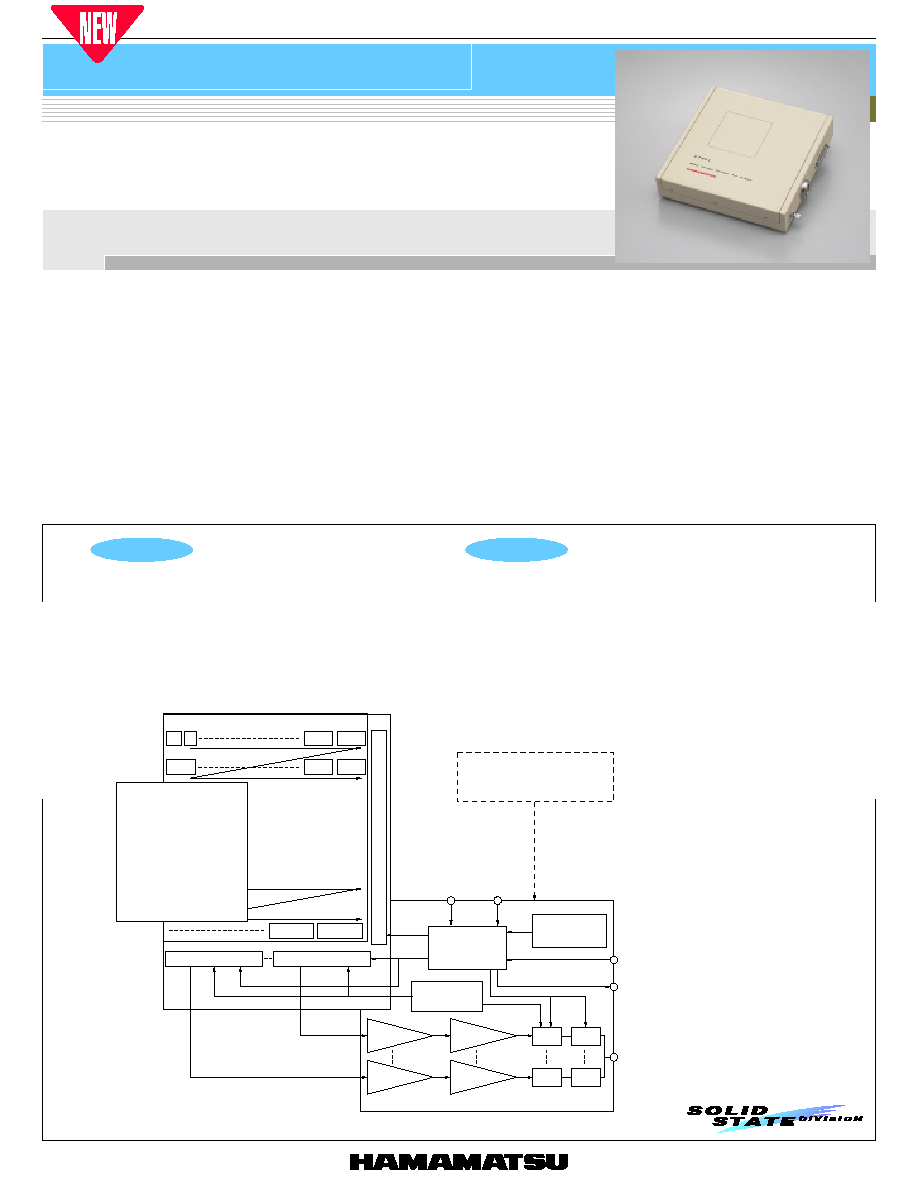
Flat panel sensor C7921 is a digital X-ray image sensor newly developed as key devices for non-destructive inspection, biomedical imaging, X-
ray microscopy and other real-time X-ray imaging applications requiring high resolution and high image quality. C7921 consists of a sensor board
and a control board, both assembled in a thin, flat and compact package. The sensor board contains a CsI scintillator plate, a two-dimensional
photodiode array with FET switches and a signal processing IC chip. The photodiode array has a 1056 × 1056 pixel format with minimized
blooming and is highly sensitive to bluish green light emitted from the CsI scintillator. Each row of pixels is addressed in sequence by the vertical
shift register connected to the gate line.
Light emission occurs when X-rays are absorbed in the CsI scintillator. This light emission enters directly into the two-dimensional photodiode
array where an electric charge is stored in each pixel according to the light intensity. This charge is then transferred to the corresponding data line
by applying a control signal to the vertical shift register.
The sensor board also has 8 charge sensitive amplifier arrays each having 132 channel amplifiers with a horizontal shift register. These amplifiers
with a total of 1056 channels are connected to a CDS (Correlated Double Sampling) circuit that senses the charge on each video line and sends it
as the analog video signal from each amplifier array. The control board converts the analog video signal into a 12-bit digital signal and outputs it to
an external frame grabber from a 12-bit parallel port.
C7921 delivers a frame rate of 16 frames per second using 4 × 4 binning and is ideal for high frame rate applications, also ideal for applications
requiring high resolution because of its 50 µm pixel size. Massive digital image data can easily be monitored on a display unit by using a frame
grabber board and video memory installed in the PC. C7921 will prove ideal tools for real-time X-ray imaging and processing where easy-to-use,
high-resolution X-ray digital image sensors are needed.
Features
l Non-destructive inspection
l Digital X-ray photography
Applications
l High quality image: 1056 × 1056 pixels
l Pixel size: 50 × 50 µm
l No image distortion
l Digital output (12 bits)
l High-speed imaging by binning operation:
16 frames/s (4 × 4 binning)
l Wide dynamic range
l High cost performance
I M A G E S E N S O R
Flat panel sensor
High resolution and high frame rate
C7921
AMP ARRAY No. 1
SHIFT REGISTER
TIMING
PULSE
GENERATOR
OSCILLATOR
ExtTrg
PIXEL NUMBER
Vsync
Hsync
Pclk
A/D
IntExt
IntExt
BINNING
(bin0, bin1)
EXTERNAL POWER SUPPLY
A. Vdd, D. Vdd V (±7.5)
(not attached)
AMP ARRAY No. 8
PHOTODIODE
ARRAY
BUFFER
AMP
BUFFER
AMP
PROCESSING
AMP
PROCESSING
AMP
1
2
1115136
1115135
1056
1055
2112
2111
1057
SCINTILLATOR
(52.8 mm × 52.8 mm)
BIAS
GENERATER
FIFO
A/D
FIFO
VIDEO OUTPUT
(12 BIT DIGITAL)
I Block diagram
KACCC0170EA
1

Flat panel sensor
C7921
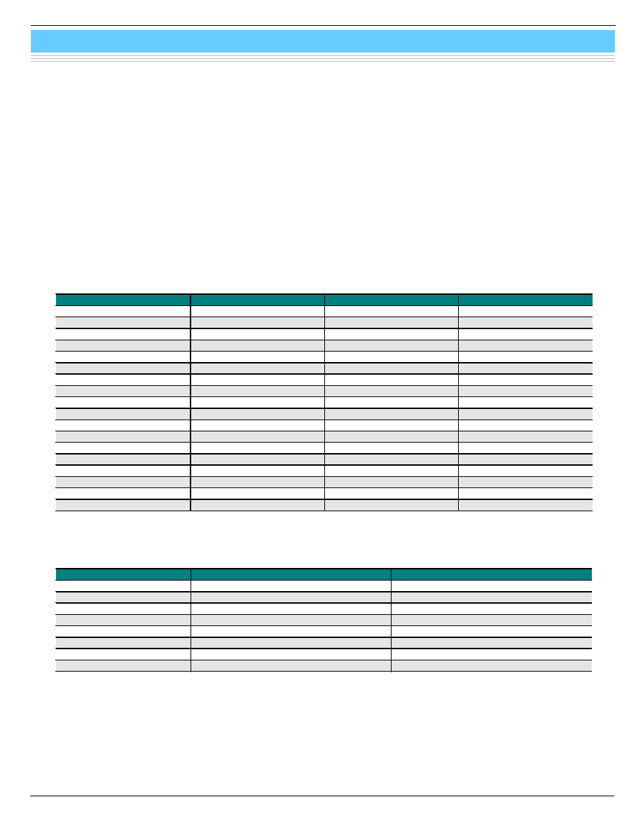
I Functional specification
Parameter
Specification
Readout
Charge amplifier array
Feedback capacitance of each amplifier
0.15 pF
Video output (Data1 - 12)
RS-422 (differential) 12 bit
Output data rate
6.25 MHz
Synchronous signal (Vsync, Hsync, Pclk)
RS-422 (differential)
bin0, 1, ExtTrg, IntExt
TTL
I Absolute maximum ratings (Ta=25 °C)
Parameter
Symbol
Value
Unit
Supply voltage for digital circuitry (+5 V)
D.vdd
+6.0
V
Supply voltage for analog circuitry (+5 V)
A.vdd
+6.0
V
Supply voltage for analog circuitry (±7.5 V)
V(+/-7.5)
±12
V
Operating temperature (not condensed)
Topr
0 to +35
°C
Storage temperature (not condensed)
Tstg
0 to +50
°C
I Specification (Unless otherwise noted, Typ. Ta=25 °C A.vdd= 5.0 V, D.vdd= 5.0 V, V (±7.5)= ±7.5 V)
Parameter
Symbol
Specification
Unit
Pixel size
-
50
µm
Active area
-
52.8 × 52.8
mm
Pixel number
-
1056 × 1056
pixels
Number of active pixels
-
1032 × 1032
pixels
Frame speed (single operation)
Sf (int)
4
frame/s
Frame speed (2 × 2 binning)
-
8
frame/s
Frame speed (4 × 4 binning)
-
16
frame/s
Frame speed external (single operation )
Sf (ext)
Sf (int) to 0.1
frame/s
Noise (rms.)
N (rms.)
1000
electrons
Saturation charge
Csat
2.9
M electrons
Resolution
Reso
8
line pairs/mm
Dynamic range
-
2900
-
Defect line *
-
10 Max.
lines
Scintillator
-
CsI
-
* Without a couple of adjacent defect line that has no response.
I Timing chart
To acquire images through an image grabber board, parameters that match the following timing chart should be described in the
software program or parameter file.
Internal mode
KACCC0167EA
Vsync+
(RS-422)
Hsync+
(RS-422)
Hsync+
(RS-422)
Pclk+
(RS-422)
Data1 - 12
(RS-422)
The number of n is 132
Tvc (1 FRAME)
Thd
Thdpw
Thc (1 LINE)
Tvdpw
Thdpw
Thc (1 LINE)
Tpd
Tpdb
Tpc (1 PIXEL)
Tppw
Tpdb
1
2
n-1
n
n+1
8n-1
8n
Tdc
Tdd
2

Flat panel sensor
C7921
External mode
KACCC0139EB
1 × 1 mode (Typ.)
Parameter
Symbol
Value
Unit
Delay time (only external trigger mode)
Tvd
450
µs
Cycle time
Tvc
243
ms
Vsync
Dummy pulse width
Tvdpw
920
µs
Delay time
Thd
2.8
µs
Cycle time
Thc
230
µs
Hsync
Dummy pulse width
Thdpw
59
µs
Delay time
Tpd
150
ns
Cycle time
Tpc
160
ns
Pulse width
Tppw
85
ns
Pclk
Delay time between each block
Tpdb
480
ns
Delay time
Tdd
50
ns
Data1-12
Cycle time
Tdc
160
ns
2 × 2 mode (Typ.)
Parameter
Symbol
Value
Unit
Delay time (only external trigger mode)
Tvd
450
µs
Cycle time
Tvc
122
ms
Vsync
Dummy pulse width
Tvdpw
920
µs
Delay time
Thd
2.8
µs
Cycle time
Thc
230
µs
Hsync
Dummy pulse width
Thdpw
140
µs
Delay time
Tpd
150
ns
Cycle time
Tpc
160
ns
Pulse width
Tppw
85
ns
Pclk
Delay time between each block
Tpdb
480
ns
Delay time
Tdd
50
ns
Data1-12
Cycle time
Tdc
160
ns
4 × 4 mode (Typ.)
Parameter
Symbol
Value
Unit
Delay time (only external trigger mode)
Tvd
450
µs
Cycle time
Tvc
62
ms
Vsync
Dummy pulse width
Tvdpw
920
µs
Delay time
Thd
2.8
µs
Cycle time
Thc
230
µs
Hsync
Dummy pulse width
Thdpw
190
µs
Delay time
Tpd
150
ns
Cycle time
Tpc
160
ns
Pulse width
Tppw
85
ns
Pclk
Delay time between each block
Tpdb
480
ns
Delay time
Tdd
50
ns
Data1-12
Cycle time
Tdc
160
ns
Note) The numbers of siginificant figures is two. (except Tvc)
RECOMMENDATION: 50 % OF FRAME TIME
FROM Tvc TO 10 s
Tvc - Tvdpw
Tvd
ExtTrg
(TTL)
Vsync+
(RS-422)
Hsync+, Pclk and Data 1-12 are the same as internal trigger mode.
3
Flat panel sensor
C7921
4
I System requirements
To operate C7921 at full performance, the following system and peripherals are required.
PC: IBM compatible PC running on Windows 98 or later operating system
Digital frame grabber card: Monochrome 16 bits or more, pixel clock 7 MHz or more, RS-422 interface synchronous signal (See
the frame grabber manual.)
The National Instruments IMAQ PCI-1424 (NI parts No. 777662-01) frame grabber has been verified to successfully acquire 12-
bit digital images from C7921. The IMAQ PCI-1422 (NI pats No. 777959-01) also acquires satisfactory images from C7921. You
can utilize the demonstration software that comes with the frame grabber as a simple viewer, to acquire and save an image. To do
so, refer to the frame grabber user's guide for how to use the camera information file for the demonstration software.
Power source: A. Vdd = +5.0 ± 0.1 V (700 mA), D. Vdd = +5.0 ± 0.1 V (800 mA), V (±7.5) = ±7.5 ± 0.5 V (±100 mA). Use of a series
power supply is recommended. (Avoid using a switching power supply.) A power cable (terminated with an FGG.2B.307.CLAD92Z
plug at one end and open at the other end; 2 m; see Table 2.) comes supplied with C7921. An optional 36-pin cable for interface
with the 36-pin receptacle (see Table 1) on C7921 is also available for synchronous signal input, video output and external
control.
The voltages described above are specified at the flat panel sensor side. The impedance of the power cable attached with the
flat panel sensor is low enough but it causes 0.1 V approx. drop. Therefore the voltage at the power source side should be set
0.1 V higher than the voltage specified above.
Table 1 Pin assignment of 36-pin receptacle
Pin No.
Signal
Pin No.
Signal
1
Data1+ (MSB)
19
Data1- (MSB)
2
Data2+
20
Data2-
3
Data3+
21
Data3-
4
Data4+
22
Data4-
5
Data5+
23
Data5-
6
Data6+
24
Data6-
7
Data7+
25
Data7-
8
Data8+
26
Data8-
9
Data9+
27
Data9-
10
Data10+
28
Data10-
11
Data11+
29
Data11-
12
Data12+(LSB)
30
Data12- (LSB)
13
bin0 (TTL)
31
Gnd
14
bin1 (TTL)
32
Gnd
15
ExtTrg (TTL)
33
IntExt (TTL)
16
Vsync+
34
Vsync-
17
Hsync+
35
Hsync-
18
Pclk+
36
Pclk-
Unless otherwise noted, signal level is RS-422.
36-pin receptacle: TX20A-36R-D2GF1-A1L made by JAE (Japan Aviation Electronics Industry limited)
36-pin mating plug: TX20A-36PH1-D2P1-D1 made by JAE (Japan Aviation Electronics Industry limited)
Table 2 Power pin assignment and cable color
Pin No.
Color
Signal
1
Brown
+7.5 V
2
Red
Analog GND
3
Orange
-7.5 V
4
Yellow
Analog GND
5
Green
Analog +5 V
6
Blue
Digital GND
7
Purple
Digital +5 V
Shield
-
Analog GND
7-pin power plug: FGG.2B.307.CLAD92Z made by LEMO S. A. (http://www.lemo.ch)
7-pin power receptacle: ECG.2B.307.CLV made by LEMO S. A.

Flat panel sensor
C7921
I Connection
Install the frame grabber board into the PC by following the manufacturer's instructions. When a general-purpose frame
grabber board is used, binning or trigger operation for bin0, bin1, IntExt and ExtTrig can be controlled with its digital I/O control.
KACCC0168EA
VIDEO OUTPUT
(12 BIT DIGITAL)
Vsync, Hsync,
Pclk
BINNING
(bin0, bin1)
IntExt
ExtTrg
X-RAY SOURCE
GRABBER
MONITOR
PC/AT
(REAR VIEW)
C7921
OS +
ACQUISITION
SOFTWARE
VOLTAGE
SOURCE
[A. Vdd, D. Vdd, V (±7.5)]
MOS Image Sensor for X-Ray
I Dimensional outline (unit: mm)
KACCA0103EA
5
142
30
142
33
MOS Image Sensor for X-Ray
C7921
33
Top cover is made of aluminum 1.0 mm thickness.
Weight: 1.37 kg
52.8
52.8
Digital Out
Power