www.gennum.com
GS9092 GenLINX® III
270Mb/s Serializer
for SDI and DVB-ASI
GS9092 Data Sheet
28202 - 2
September 2005
1 of 58
Key Features
·
SMPTE 259M-C compliant scrambling and NRZI to
NRZ encoding (with bypass)
·
DVB-ASI sync word insertion and 8b/10b encoding
·
Integrated Cable Driver
·
Integrated line-based FIFO for data
alignment/delay, clock phase interchange, DVB-ASI
data packet insertion, and ancillary data packet
insertion
·
User selectable additional processing features
including:
· ANC data checksum, and line number
calculation and insertion
· TRS and EDH packet generation and insertion
· illegal code remapping
·
Enhanced Gennum Serial Peripheral Interface
(GSPI)
·
JTAG test interface
·
+1.8V internal cable driver and core power supply
·
Optional +1.8V or +3.3V digital I/O power supply
·
Small footprint (8mm x 8mm)
·
Low power operation (typically 170mW)
·
Pb-free and RoHS compliant
Applications
·
SMPTE 259M-C Serial Digital Interfaces
·
DVB-ASI Serial Digital Interfaces
Description
The GS9092 is a 270Mb/s serializer with an internal
FIFO and an integrated cable driver. It contains all the
necessary blocks to realize a transmit solution for
SD-SDI and DVB-ASI applications.
In addition to serializing the input data stream, the
GS9092 performs NRZI-to-NRZ encoding and
scrambling as per SMPTE 259M-C when operating in
SMPTE mode. When operating in DVB-ASI mode, the
device will insert K28.5 sync characters and 8b/10b
encode the data prior to serialization.
Parallel data inputs are provided for 10-bit multiplexed
formats at SD signal rates. A 27MHz parallel clock input
signal is also required.
The integrated cable driver features an adjustable
signal swing and common mode operating point offering
fully compliant SMPTE 259M-C cable driver
connectivity.
The GS9092 includes a range of data processing
functions such as automatic standards detection and
EDH support. The device can also insert TRS signals,
re-map illegal code words, and generate and insert
SMPTE 352M payload identifier packets. All processing
features are optional and may be enabled/disabled via
external control pin(s) and/or host interface
programming.
The GS9092 also incorporates a video line-based FIFO.
This FIFO may be used in four user-selectable modes
to carry out tasks such as data delay, clock phase
interchange, MPEG packet insertion and clock rate
interchange, and ancillary data packet insertion.
The device may also be used as a low-latency
parallel-to-serial converter where the SMPTE
scrambling block will be the only processing feature
enabled.
The GS9092 is Pb-free, and the encapsulation
compound does not contain halogenated flame
retardant (RoHS compliant).

GS9092 Data Sheet
28202 - 2
September 2005
3 of 58
Contents
Key Features.................................................................................................................1
Applications...................................................................................................................1
Description ....................................................................................................................1
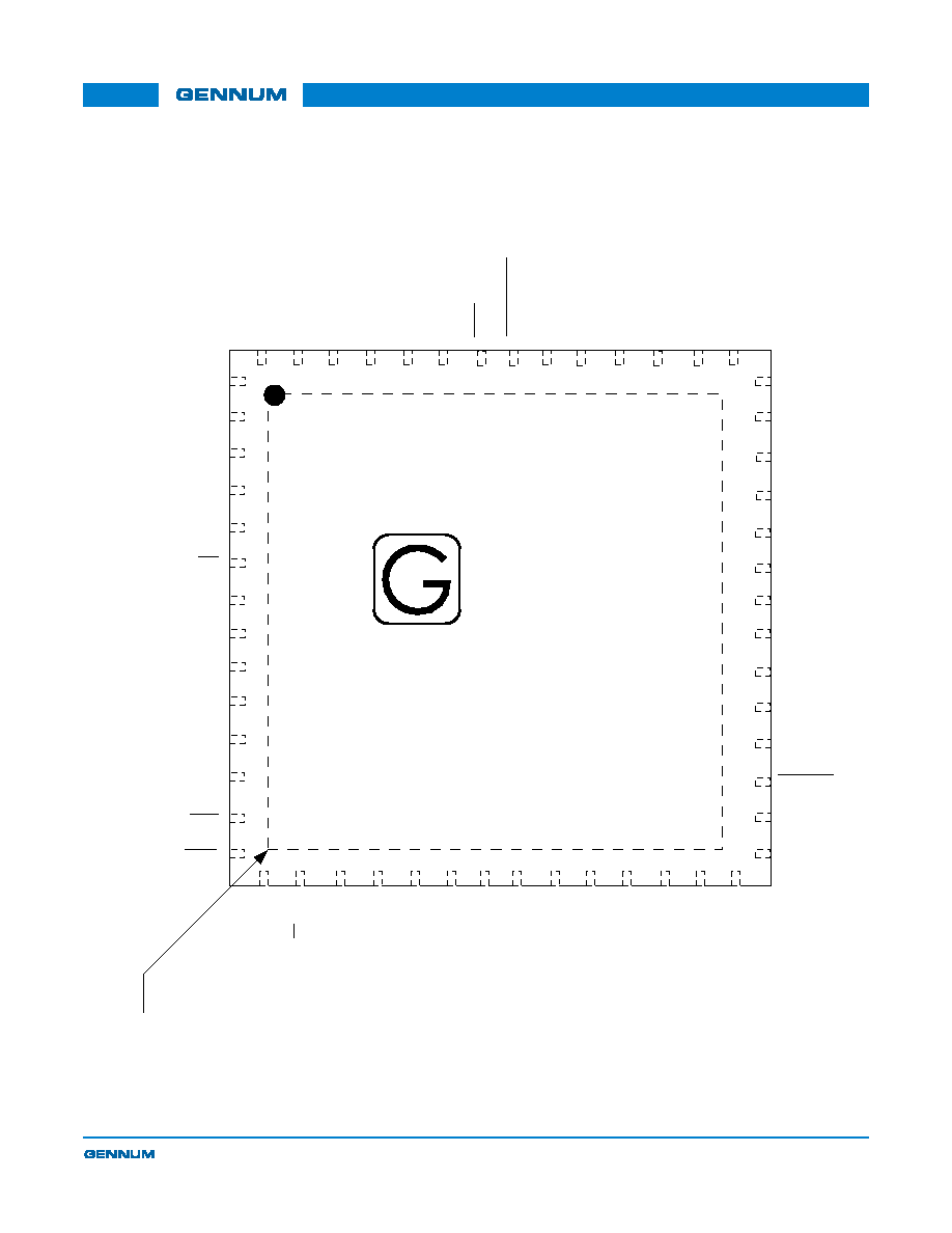
1. Pin Out .....................................................................................................................5
1.1 Pin Assignment ...............................................................................................5
1.2 Pin Descriptions ..............................................................................................6
2. Electrical Characteristics........................................................................................11
2.1 Absolute Maximum Ratings ..........................................................................11
2.2 DC Electrical Characteristics ........................................................................12
2.3 AC Electrical Characteristics.........................................................................13
2.4 Solder Reflow Profiles...................................................................................15
2.5 Host Interface Maps......................................................................................16
2.5.1 Host Interface Map (Read only registers) ...........................................17
2.5.2 Host Interface Map (R/W configurable registers)................................18
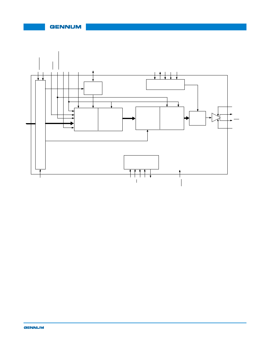
3. Detailed Description ...............................................................................................19
3.1 Functional Overview .....................................................................................19
3.2 Parallel Data Inputs.......................................................................................20
3.2.1 Parallel Input in SMPTE Mode............................................................21
3.2.2 Parallel Input in DVB-ASI Mode..........................................................21
3.2.3 Parallel Input in Data-Through Mode..................................................21
3.2.4 I/O Buffers...........................................................................................21
3.3 Internal FIFO Operation ................................................................................22
3.3.1 Video Mode.........................................................................................23
3.3.2 DVB-ASI Mode ...................................................................................24
3.3.3 Ancillary Data Insertion Mode.............................................................28
3.3.4 Bypass Mode ......................................................................................32
3.4 SMPTE Mode................................................................................................32
3.4.1 I/O Status Signals ...............................................................................32
3.4.2 HVF Timing Signal Inputs ...................................................................32
3.5 DVB-ASI Mode..............................................................................................33
3.5.1 Control Signal Inputs ..........................................................................33
3.6 Data-Through Mode......................................................................................34
3.7 Additional Processing Functions...................................................................34
3.7.1 Input Data Blank .................................................................................34
3.7.2 Automatic Video Standard Detection..................................................34
3.7.3 Packet Generation and Insertion ........................................................35
3.8 Parallel-to-Serial Conversion ........................................................................45
3.9 Serial Digital Data PLL..................................................................................45
3.10 Serial Digital Output ....................................................................................46
3.10.1 Output Swing ....................................................................................46

GS9092 Data Sheet
28202 - 2
September 2005
4 of 58
3.10.2 Serial Digital Output Mute Control ....................................................46
3.11 Programmable Multi-function I/O ................................................................46
3.12 GS9092 Low Latency Mode........................................................................48
3.13 GSPI Host Interface ....................................................................................49
3.13.1 Command Word Description.............................................................50
3.13.2 Data Read and Write Timing ............................................................50
3.13.3 Configuration and Status Registers ..................................................52
3.14 JTAG Operation ..........................................................................................53
3.15 Device Power Up ........................................................................................54
4. References & Relevant Standards.........................................................................54
5. Application Information...........................................................................................55
5.1 Typical Application Circuit.............................................................................55
6. Package & Ordering Information............................................................................56
6.1 Package Dimensions ....................................................................................56
6.2 Recommended PCB Footprint ......................................................................57
6.3 Packaging Data.............................................................................................57
6.4 Ordering Information .....................................................................................57
7. Revision History .....................................................................................................58