UG06A thru UG06D
Vishay Semiconductors
formerly General Semiconductor
Document Number 88757
www.vishay.com
14-Feb-02
1
Miniature Ultrafast Plastic Rectifier
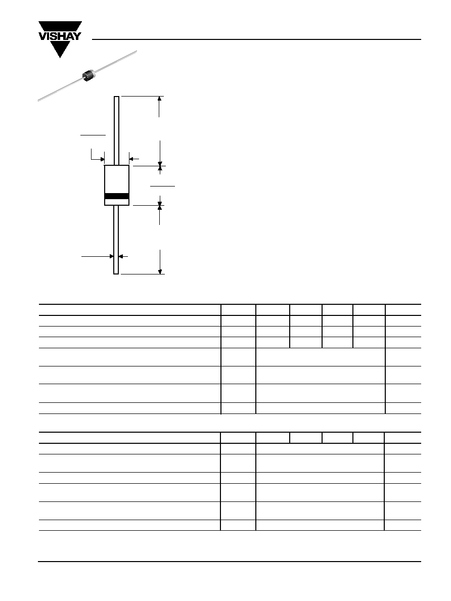
1.0 (25.4)
MIN.
1.0 (25.4)
MIN.
0.125 (3.18)
0.115 (2.92)
0.100 (2.54)
0.090 (2.29)
0.025 (0.635)
0.023 (0.584)
DIA
DIA.
MPG06
Maximum Ratings & Thermal Characteristics
Ratings at 25°C ambient temperature unless otherwise specified.
Parameters
Symbols
UG06A
UG06B
UG06C
UG06D
Units
Maximum repetitive peak reverse voltage
V
RRM
50
100
150
200
V
Maximum RMS voltage
V
RMS
35
70
105
140
V
Maximum DC blocking voltage
V
DC
50
100
150
200
V
Maximum average forward rectified current at 0.375"
I
F(AV)
0.6
A
(9.5mm) lead length at T
L
= 75şC
Peak forward surge current 8.3 ms single half sine-wave
I
FSM
40
A
superimposed on rated load (JEDEC Method) at T
L
= 75şC
Typical thermal resistance
(1)
R
JA
97
°C/W
R
JL
28
Operating junction and storage temperature range
T
J
, T
STG
-55 to +150°C
°C
Electrical Characteristics
Ratings at 25°C ambient temperature unless otherwise specified.
Parameters
Symbols
UG06A
UG06B
UG06C
UG06D
Units
Maximum instantaneous forward voltage at 0.6A
V
F
0.95
V
Maximum DC reverse current
T
A
= 25°C
I
R
5.0
µ
A
at rated DC blocking voltage
T
A
=100°C
100
Maximum reverse recovery time at I
F
=0.5A, I
R
=1.0A, I
rr
=0.25A
t
rr
15
ns
Maximum reverse recovery time
T
J
= 25°C
t
rr
25
ns
I
F
=0.6A, V
R
=30V, di/dt=50A/
µ
s, I
rr
=10% I
RM
T
J
= 100°C
35
Maximum recovered stored charge
T
J
= 25°C
Q
rr
8.0
nC
I
F
=0.6A, V
R
=30V, di/dt=50A/
µ
s, I
rr
=10% I
RM
T
J
= 100°C
20
Typical junction capacitance at 4V, 1MHz
C
J
9.0
pF
Notes: (1) Thermal resistance from junction to ambient and junction to lead at 0.375" (9.5mm) lead length
P.C.B. mounted with 0.2 x 0.2" (5.0 x 5.0mm) copper pads
(2) Pulse test: 300
µ
s pulse width, 1% duty cycle
Dimensions in inches and (millimeters)
Features
· Plastic package has Underwriters Laboratories
Flammability Classification 94V-0
· Ideally suited for use in very high frequency switching
power supplies, inverters and as free wheeling diodes
· Ultrafast recovery time for high efficiency
· Excellent high temperature switching
· Soft recovery characteristics
· Glass passivated junction
· High temperature soldering guaranteed:
250°C/10 seconds, 0.375" (9.5mm) lead length,
5 lbs. (2.3kg) tension
Mechanical Data
Case: Void free molded plastic body over glass
passivated chip
Terminals: Plated axial leads, solderable per
MIL-STD-750, Method 2026
Polarity: Color band denotes cathode end
Mounting Position: Any
Weight: 0.0064 oz., 0.181 g
Reverse Voltage 50 to 200V
Forward Current 0.6A
UG06A thru UG06D
Vishay Semiconductors
formerly General Semiconductor
www.vishay.com
Document Number 88757
2
14-Feb-02
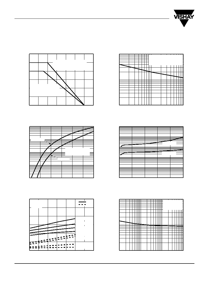
Ratings and
Characteristic Curves
(T
A
= 25°C unless otherwise noted)
Temperature (
°
C)
Fig. 1 -- Maximum Forward Current
Derating Curves
A
verage Forward Rectified Current (A)
Fig. 3 -- Typical Instantaneous
Forward Characteristics
Instantaneous Forward Voltage (V)
Instantaneous Forward Current (A)
Percent of Rated Peak Reverse Voltage (%)
Instantaneous Reverse Leakage
Current (
µ
A)
Fig. 4 -- Typical Reverse Leakage
Characteristics
Fig. 6 -- Typical Junction Capacitance
Number of Cycles at 60 H
Z
Reverse Voltage (V)
Fig. 2 -- Maximum Non-Repetitive
Peak Forward Surge Current
Peak Forward Surge Current (A)
Junction Temperature (
°
C)
Recovered Charge / Reverse Recovery
T
ime, nC/ns
Junction Capacitance, pF
Fig. 5 -- Reverse Switching
Characteristics
0
25
50
75
100
125
150
175
0
0.15
0.3
0.45
0.6
0.75
0.9
Resistive or Inductive Load
0.375" (9.5mm) Lead Length
T
L
Lead Temperature
T
A
, Ambient Temperature
P.C.B. Mounted
0.2" x 0.2" (5 x 5mm)
Copper Pads
1
10
100
1
10
100
T
J
= 75
°
C
8.3ms Single Half Sine-Wave
(JEDEC Method)
0.4
0.6
0.8
1.0
1.2
1.4
1.6
0.01
0.1
1
10
100
T
J
= 100
°
C
T
J
= 25
°
C
Pulse Width = 300
µ
s
1% Duty Cycle
0
20
40
60
80
100
0.01
0.1
1
10
100
1,000
0
25
50
75
100
125
150
175
0
10
20
30
40
50
60
I
F
= 0.6A
V
R
=30V
t
rr
Q
rr
di/dt=20A/
µ
s
di/dt=150A/
µ
s
di/dt=100A/
µ
s
di/dt=50A/
µ
s
di/dt=150A/
µ
s
di/dt=100A/
µ
s
di/dt=20A/
µ
s
di/dt=50A/
µ
s
0.1
1
10
100
1
10
100
T
J
= 25
°
C
f = 1.0MH
Z
Vsig = 50mVp-p
T
J
= 100
°
C
T
J
= 25
°
C