
FEATURES
MECHANICAL DATA
Case: TO-92 Plastic Package
Weight: approx. 0.18 g
MAXIMUM RATINGS AND ELECTRICAL CHARACTERISTICS
Small Signal Transistors (PNP)
B
C
E
.181 (4.6)
mi
n. .492
(
12.5)
.181 (
4
.6)
.142 (3.6)
Dimensions in inches and (millimeters)
TO-92
Ratings at 25 °C
ambient temperature unless otherwise specified
.098 (2.5)
max.
.022 (0.55)
4/98
MPSA92, MPSA93
PNP Silicon Epitaxial Planar Tran-
sistors especially suited as line
switch in telephone subsets
and in video output stages of
TV receivers and monitors.
As complementary types, the PNP
transistors MPSA42 and MPSA43 are
recommended.
Symbol
Value
Unit
Collector-Emitter Voltage
MPSA92
MPSA93
V
CEO
V
CEO
300
200
V
V
Collector-Base Voltage
MPSA92
MPSA93
V
CBO
V
CBO
300
200
V
V
Emitter-Base Voltage
V
EBO
5
V
Collector Current
I
C
500
mA
Power Dissipation at T
amb
= 25 °C
P
tot
625
1)
mW
Junction Temperature
T
j
150
°C
Storage Temperature Range
T
S
65 to +150
°C
1)
Valid provided that lead are kept at ambient temperature at a distance of 2 mm from case.
Absolute Maximum Ratings
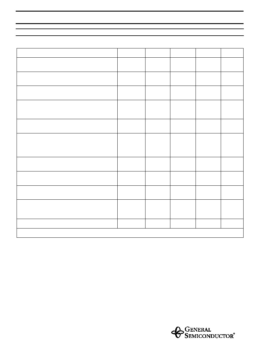
ELECTRICAL CHARACTERISTICS
Ratings at 25 °C
ambient temperature unless otherwise specified
MPSA92, MPSA93
Symbol
Min.
Typ.
Max.
Unit
Collector-Emitter Breakdown Voltage
MPSA92
I
C
= 10 mA, I
B
= 0
MPSA93
V
(BR)CEO
V
(BR)CEO
300
200
V
V
Collector-Base Breakdown Voltage
MPSA92
I
C
= 100
µ
A, I
E
= 0
MPSA93
V
(BR)CBO
V
(BR)CBO
300
200
V
V
Emitter-Base Breakdown Voltage
I
E
= 100
µ
A, I
C
= 0
V
(BR)EBO
5
V
Collector-Base Cutoff Current
V
CB
= 200 V, I
E
= 0
MPSA92
V
CB
= 160 V, I
E
= 0
MPSA93
I
CBO
I
CBO
250
250
nA
nA
Emitter-Base Cutoff Current
V
EB
= 3 V, I
C
= 0
I
EBO
100
nA
DC Current Gain
I
C
= 1 mA, V
CE
= 10 V
I
C
= 10 mA, V
CE
= 10 V
I
C
= 30 mA, V
CE
= 10 V
h
FE
h
FE
h
FE
25
40
25
Collector-Emitter Saturation Voltage
I
C
= 20 mA, I
B
= 2 mA
V
CEsat
500
mV
Base-Emitter Saturation Voltage
I
C
= 20 mA, I
B
= 2 mA
V
BEsat
900
mV
Gain-Bandwidth Product
I
C
= 10 mA, V
CE
= 20 V, f = 100 MHz
f
T
50
MHz
Collector-Base Capacitance
V
CB
= 20 V, I
E
= 0, f = 1 MHz
MPSA92
MPSA93
C
CBO
C
CBO
6
8
pF
pF
Thermal Resistance Junction to Ambient Air
R
thJA
200
1)
K/W
1)
Valid provided that lead are kept at ambient temperature at a distance of 2 mm from case.