FEATURES
DMOS Transistors (P-Channel)
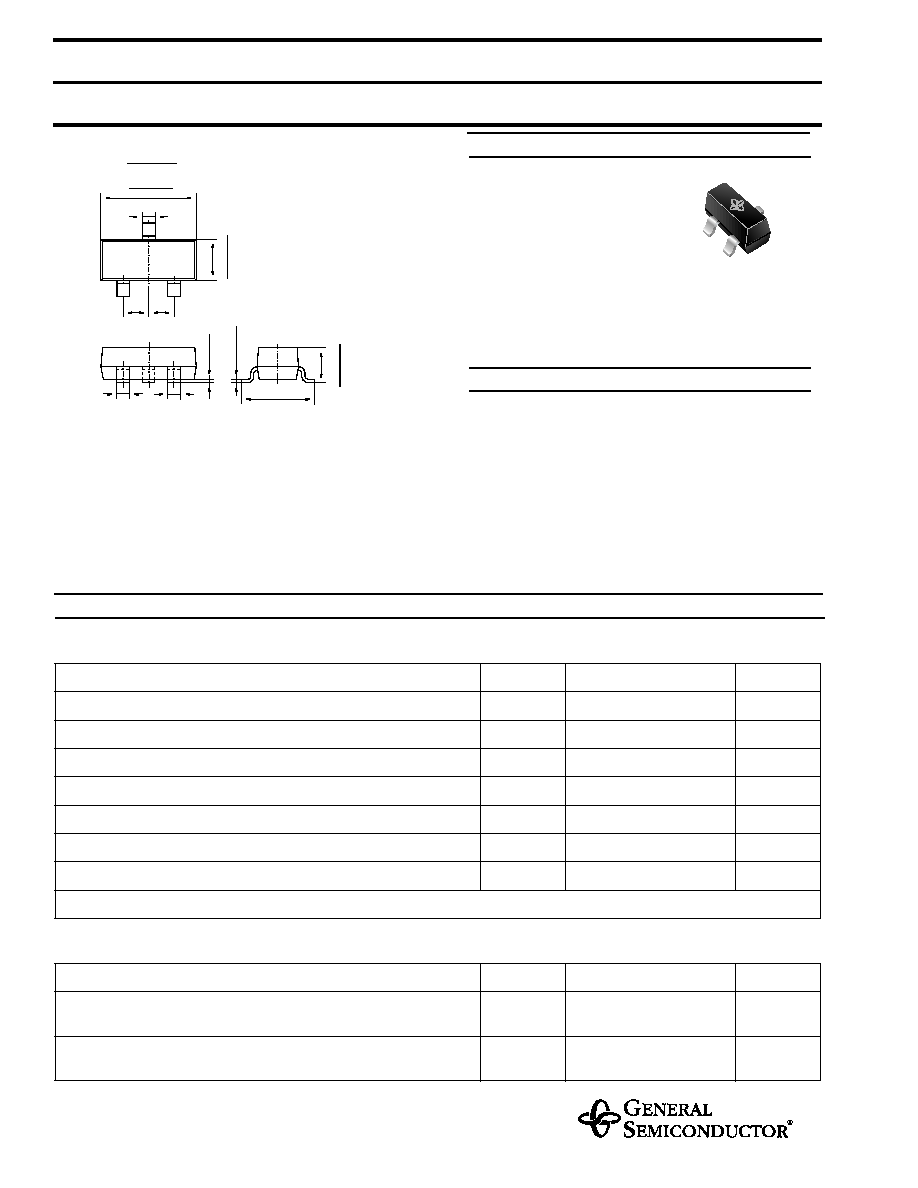
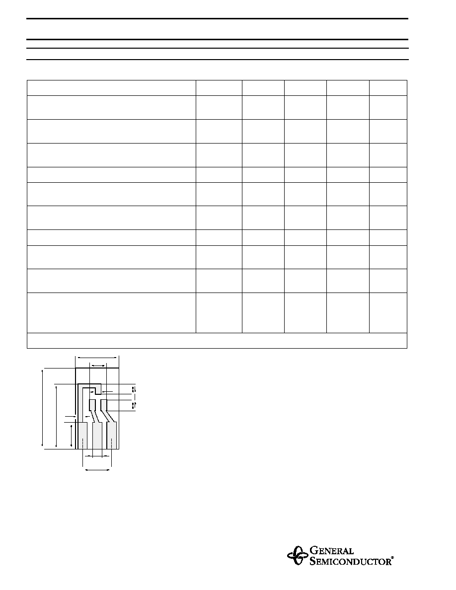
Dimensions in inches and (millimeters)
.016 (0.4)
.056
(
1
.43
)
.037(0.95) .037(0.95)
max
.
.004 (
0
.1)
.122 (3.1)
.016 (0.4)
.016 (0.4)
3
1
2
Top View
.102 (2.6)
.007 (
0
.175)
.045 (
1
.15)
.118 (3.0)
.052
(
1
.3
3
)
.005 (
0
.125)
.094 (2.4)
.037 (
0
.95)
Case: SOT-23 Plastic Package
Weight: approx. 0.008 g
MECHANICAL DATA
MAXIMUM RATINGS AND ELECTRICAL CHARACTERISTICS
Ratings at 25 °C
ambient temperature unless otherwise specified
Pin configuration
1 = Gate, 2 = Source, 3 = Drain
SOT-23
4/98
BS850
Inverse Diode
Symbol
Value
Unit
Drain-Source Voltage
V
DSS
60
V
Drain-Gate Voltage
V
DGS
60
V
Gate-Source Voltage (pulsed)
V
GS
± 20
V
Drain Current (continuous)
I
D
250
mA
Power Dissipation at T
SB
= 50 °C
P
tot
0.310
1)
W
Junction Temperature
T
j
150
°C
Storage Temperature Range
T
S
65 to +150
°C
1)
Device on fiberglass substrate, see layout
Symbol
Value
Unit
Max. Forward Current (continuous)
at T
amb
= 25 °C
I
F
0.3
A
Forward Voltage Drop (typ.)
at V
GS
= 0, I
F
= 0.12 A, T
j
= 25 °C
V
F
0.85
V
Marking
S50
High input impedance
High-speed switching
No minority carrier storage time
CMOS logic compatible input
No thermal runaway
No secondary breakdown
ELECTRICAL CHARACTERISTICS
Ratings at 25 °C
ambient temperature unless otherwise specified
BS850
Symbol
Min.
Typ.
Max.
Unit
Drain-Source Breakdown Voltage
at I
D
= 100
µ
A, V
GS
= 0
V
(BR)DSS
60
90
V
Gate Threshold Voltage
at V
GS
= V
DS
, I
D
= 1 mA
V
GS(th)
1.0
2
3.0
V
Gate-Body Leakage Current
at V
GS
= 15 V, V
DS
= 0
I
GSS
10
nA
Drain Cutoff Current at V
DS
= 25 V, V
GS
= 0
I
DSS
0.5
µ
A
Drain-Source ON Resistance
at V
GS
= 10 V, I
D
= 200 mA
R
DS(ON)
3.5
5.0
Thermal Resistance Junction to Substrate
Backside
R
thSB
320
1)
K/W
Thermal Resistance Junction to Ambient Air
R
thJA
450
1)
K/W
Forward Transconductance
at V
DS
= 10 V, I
D
= 200 mA, f = 1 MHz
g
m
200
mS
Input Capacitance
at V
DS
= 10 V, V
GS
= 0, f = 1 MHz
C
iss
60
pF
Switching Times
at V
GS
= 10 V, V
DS
= 10 V, R
D
= 100
Turn-On Time
Turn-Off Time
t
on
t
off
5
25
ns
ns
1)
Device on fiberglass substrate, see layout
.59 (15)
0.2 (5)
.03 (0.8)
.30 (7.5)
.12 (3)
.04 (1)
.06 (1.5)
.20 (5.1)
.08 (2)
.08 (2)
.04 (1)
Dimensions in inches (millimeters)
.47 (12)
Layout for R
thJA
test
Thickness: Fiberglass 0.059 in (1.5 mm)
Copper leads 0.012 in (0.3 mm)