FEATURES
Small Signal Transistors (PNP)
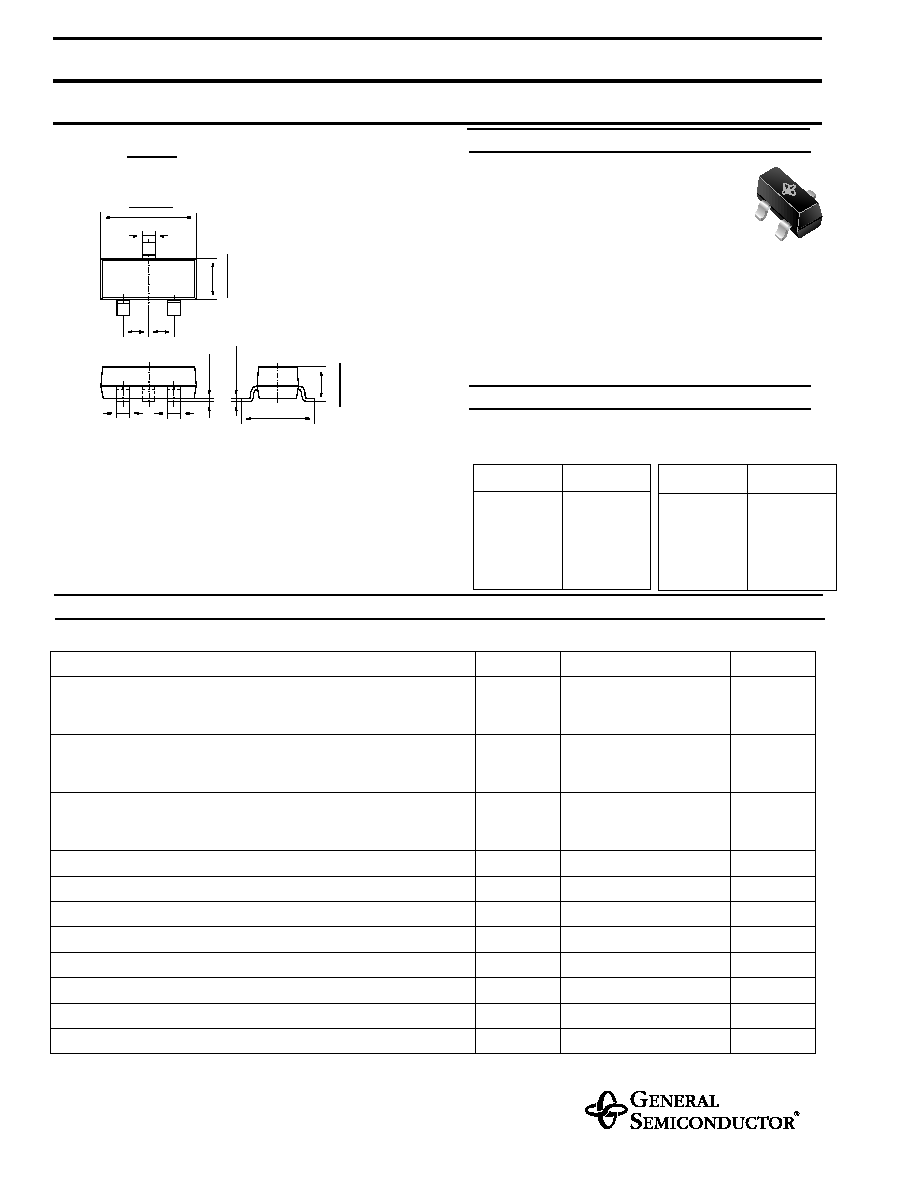
Dimensions in inches and (millimeters)
.016 (0.4)
.056 (
1
.43
)
.037(0.95) .037(0.95)
ma
x
.
.004
(
0
.1
)
.122 (3.1)
.016 (0.4)
.016 (0.4)
3
1
2
Top View
.102 (2.6)
.007 (
0
.17
5
)
.0
45 (
1
.15)
.118 (3.0)
.052 (
1
.33
)
.005
(
0
.1
25)
.094 (2.4)
.0
37 (
0
.95)
Case: SOT-23 Plastic Package
Weight: approx. 0.008 g
MECHANICAL DATA
MAXIMUM RATINGS AND ELECTRICAL CHARACTERISTICS
Ratings at 25 °C
ambient temperature unless otherwise specified
Pin configuration
1 = Base, 2 = Emitter, 3 = Collector.
SOT-23
4/98
Marking code
Type
Marking
BC856A
B
BC857A
B
C
BC858A
B
C
3A
3B
3E
3F
3G
3J
3K
3L
Symbol
Value
Unit
Collector-Base Voltage
BC856
BC857
BC858, BC859
V
CBO
V
CBO
V
CBO
80
50
30
V
V
V
Collector-Emitter Voltage
BC856
BC857
BC858, BC859
V
CES
V
CES
V
CES
80
50
30
V
V
V
Collector-Emitter Voltage
BC856
BC857
BC858, BC859
V
CEO
V
CEO
V
CEO
65
45
30
V
V
V
Emitter-Base Voltage
V
EBO
5
V
Collector Current
I
C
100
mA
Peak Collector Current
I
CM
200
mA
Peak Base Current
I
BM
200
mA
Peak Emitter Current
I
EM
200
mA
Power Dissipation at T
SB
= 50 °C
P
tot
310
1)
mW
Junction Temperature
T
j
150
°C
Storage Temperature Range
T
S
65 to +150
°C
Type
Marking
BC859A
B
C
4A
4B
4C
PNP Silicon Epitaxial Planar Transistors
for switching and AF amplifier applications.
Especially suited for automatic insertion in
thick- and thin-film circuits.
These transistors are subdivided into three groups A, B
and C according to their current gain. The type BC856 is
available in groups A and B, however, the types BC857,
BC858 and BC859 can be supplied in all three groups.
The BC859 is a low noise type.
As complementary types, the NPN transistors
BC846 ... BC849 are recommended.
BC856 THRU BC859

ELECTRICAL CHARACTERISTICS
Ratings at 25 °C
ambient temperature unless otherwise specified
Symbol
Min.
Typ.
Max.
Unit
h-Parameters
at V
CE
= 5 V, I
C
= 2 mA, f = 1 kHz
Current Gain
Current Gain Group A
B
C
Input Impedance
Current Gain Group A
B
C
Output Admittance
Current Gain Group A
B
C
Reverse Voltage Transfer Ratio
Current Gain Group A
B
C
h
fe
h
fe
h
fe
h
ie
h
ie
h
ie
h
oe
h
oe
h
oe
h
re
h
re
h
re
1.6
3.2
6
220
330
600
2.7
4.5
8.7
18
30
60
1.5 · 10
4
2 · 10
4
3 · 10
4
4.5
8.5
15
30
60
110
k
k
k
µ
S
µ
S
µ
S
DC Current Gain
at V
CE
= 5 V, I
C
= 10
µ
A
Current Gain Group A
B
C
at V
CE
= 5 V, I
C
= 2 mA
Current Gain Group A
B
C
h
FE
h
FE
h
FE
h
FE
h
FE
h
FE
110
200
420
90
150
270
180
290
520
220
450
800
Thermal Resistance Junction to Substrate
Backside
R
thSB
320
1)
K/W
Thermal Resistance Junction to Ambient Air
R
thJA
450
1)
K/W
Collector Saturation Voltage
at I
C
= 10 mA, I
B
= 0.5 mA
at I
C
= 100 mA, I
B
= 5 mA
V
CEsat
V
CEsat
90
250
300
650
mV
mV
Base Saturation Voltage
at I
C
= 10 mA, I
B
= 0.5 mA
at I
C
= 100 mA, I
B
= 5 mA
V
BEsat
V
BEsat
700
900
mV
mV
Base-Emitter Voltage
at V
CE
= 5 V, I
C
= 2 mA
at V
CE
= 5 V, I
C
= 10 mA
V
BE
V
BE
600
660
750
800
mV
mV
Collector-Emitter Cutoff Current
at V
CE
= 80 V
BC856
at V
CE
= 50 V
BC857
at V
CE
= 30 V
BC858, BC859
at V
CE
= 80 V, T
j
= 125 °C
BC856
at V
CE
= 50 V, T
j
= 125 °C
BC857
at V
CE
= 30 V, T
j
= 125 °C
BC858, BC859
at V
CB
= 30 V
at V
CB
= 30 V, T
j
= 150 °C
I
CES
I
CES
I
CES
I
CES
I
CES
I
CES
I
CBO
I
CBO
0.2
0.2
0.2
15
15
15
4
4
4
15
5
nA
nA
nA
µ
A
µ
A
µ
A
nA
µ
A
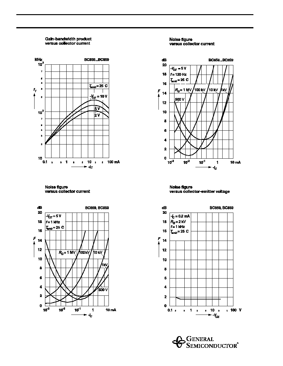
Gain-Bandwidth Product
at V
CE
= 5 V, I
C
= 10 mA, f = 100 MHz
f
T
150
MHz
1)
Device on fiberglass substrate, see layout
BC856 THRU BC859
ELECTRICAL CHARACTERISTICS
Ratings at 25 °C
ambient temperature unless otherwise specified
Symbol
Min.
Typ.
Max.
Unit
Collector-Base Capacitance
at V
CB
= 10 V, f = 1 MHz
C
CBO
6
pF
Noise Figure
at V
CE
= 5 V, I
C
= 200
µ
A, R
G
= 2 k
,
f = 1 kHz,
f = 200 Hz
BC856, BC857, BC858
BC859
F
F
2
1
10
4
dB
dB
Noise Figure
at V
CE
= 5 V, I
C
= 200
µ
A, R
G
= 2 k
,
f = 30... 15000 Hz
BC859
F
1.2
4
dB
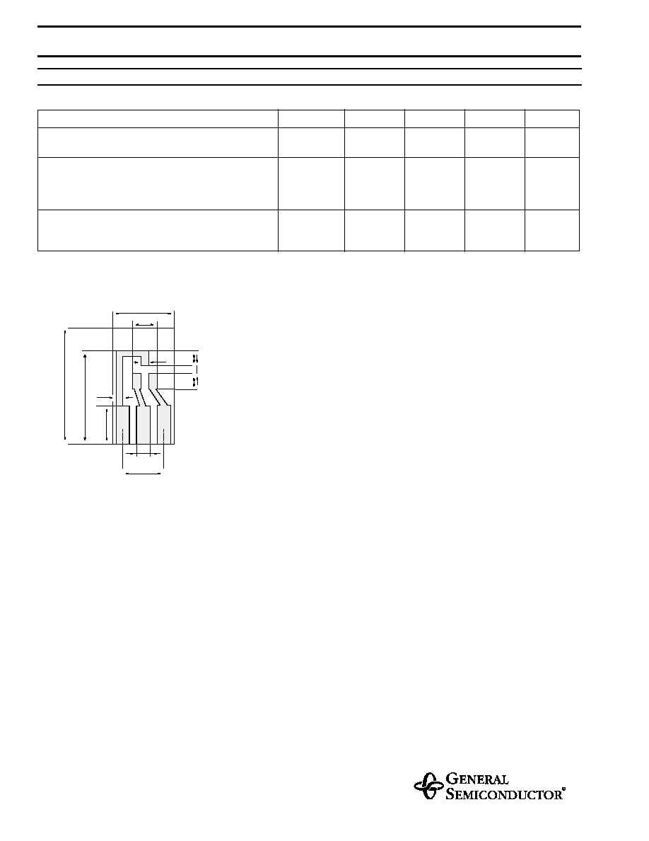
BC856 THRU BC859
Layout for R
thJA
test
Thickness: Fiberglass 0.059 in (1.5 mm)
Copper leads 0.012 in (0.3 mm)
.59 (15)
0.2 (5)
.03 (0.8)
.30 (7.5)
.12 (3)
.04 (1)
.06 (1.5)
.20 (5.1)
.08 (2)
.08 (2)
.04 (1)
Dimensions in inches (millimeters)
.47 (12)

Collector-base cutoff current
versus junction temperature
nA
-I
CBO
10
100
0
1
T
j
200
°
C
BC856...BC859
10
3
10
4
10
2
10
-1
Test voltage -V :
equal to the given
maximum value
typical
maximum
-V
CEO
CBO
RATINGS AND CHARACTERISTIC CURVES BC856 THRU BC859

Collector current
versus base-emitter voltage
mA
10
5
-I
C
10
1
0
10
-V
BE
BC856...BC859
2
4
3
2
5
4
3
2
5
4
3
2
-1
0.5
1 V
-V
CE
= 5 V
T
amb
= 25
°
C
Collector saturation voltage
versus collector current
V
0.5
0.4
-V
CEsat
0.3
0.2
1
0
0.1
-I
C
BC856...BC859
10
2
5
2
5
2
5
10
-1
10 mA
2
-50
°
C
-I
C
= 20
-I
B
T
amb =
100
°
C
25
°
C
RATINGS AND CHARACTERISTIC CURVES BC856 THRU BC859
RATINGS AND CHARACTERISTIC CURVES BC856 THRU BC859