ICS1738
QuickSaver® Pulse Conditioning Charge Control IC for
Rechargeable Lithium-Ion Batteries
General Description
The ICS1738 is a low cost 8 pin CMOS IC that provides a unique pulse conditioning charge technique, precision reference,
fast charge time-out, back-up over-voltage and under-voltage shutdown, and status indicator for charging single and multiple
cell rechargeable lithium-ion battery packs. The ICS1738 uses a pulsed charging technique with an option to interleave brief
discharge pulses as part of the charging process for maximizing battery performance and service life span. While pauses in the
charging process alone provide some improvement in battery performance compared to constant unidirectional charging,
maximum battery performance is gained by incorporating the brief discharge pulse option. Discharge pulse conditioning
produces the highest level of charge by increasing charge acceptance and at the same time reduces voltage induced
intercalation that causes battery capacity fade, internal series resistance build-up, and internal shunt resistance decline.
Discharge pulse conditioning removes surface charge from cell electrodes preventing premature arrival at minimum current
levels most often used to terminate fast charge with limited current to fixed voltage charging methods. By removing surface
charge, discharge pulse conditioning reduces lithium-ion's inherent propensities of internal resistance build-up and capacity
loss capacity with use (capacity fade). Discharge pulse conditioning causes a more uniform distribution of charge into the cell
electrode surface resulting in less internal drop during discharge and reduced battery self-discharge. The ICS1738 is for use
with battery packs that have active and passive current, voltage, and thermal protection required by the cell's manufacturer.
Applications
Embedded and charger stands: Portable, handheld products/equipment: PDA, computer, POS, audio/video, wireless, etc.
Features
· Fast charge termination methods: Designer configured minimum current and/or settable fast charge time limit
· Four stage charge sequence: Soft Start Conditioning, Fast charge, Topping charge, and Maintenance charge
· User accessible clock and voltage reference; optional discharge pulse conditioning, back-up over/under voltage shutdown
Benefits
products compared to other charge methods
· Peak charge level and extended battery service life span; markedly improve product performance, efficiency, reliability
· Lower capacity fade and lower internal series resistance build-up eliminates or lessens dependence on spare batteries
· Less internal shunt resistance decline (battery self discharge) provides improved sleep/store mode capacity retention
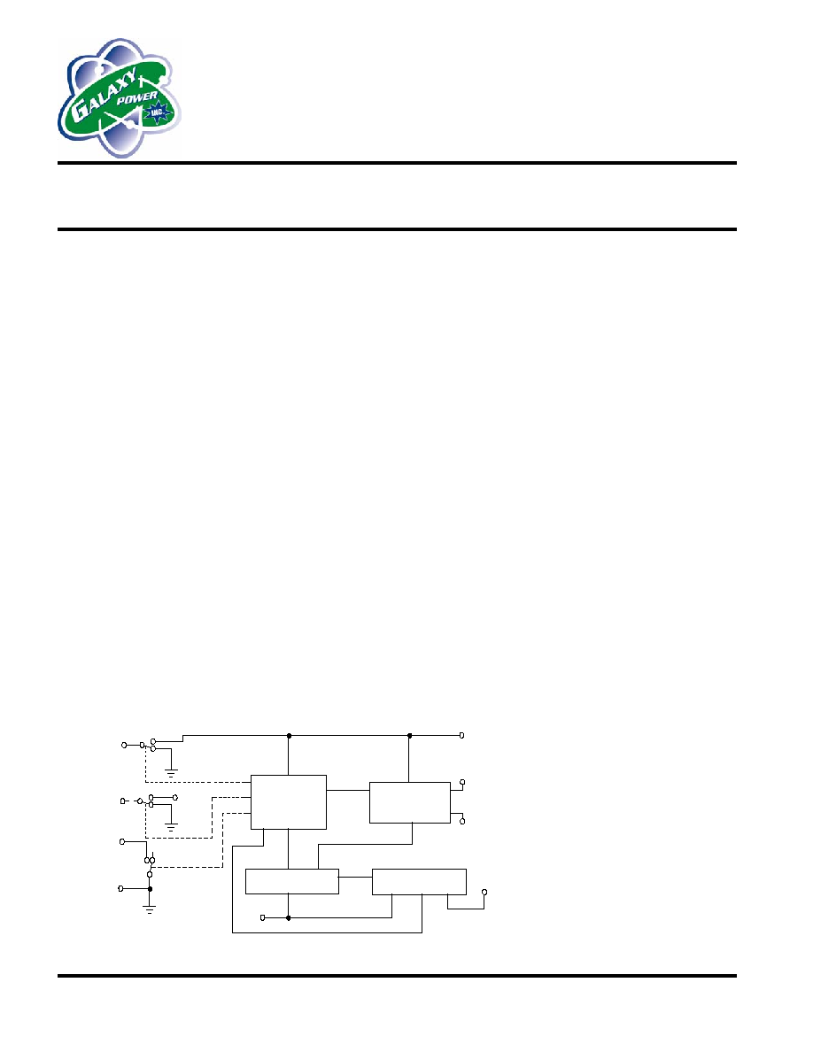
Device I/O Diagram
VSS pin 4
CMN pin 3
ON
OFF
OFF
VDD
OFF
ON
DCHG pin 2
CHG pin 1
VDD pin 8
VIN pin 7
VREF pin 6
RC pin 5
COMPARATOR
A TO D
BAND GAP
PULSE/TIME
CONTROL AND
DRIVES
PROCESSOR
OSCILLATOR
VDD

2
ICS1738
Pin Configuration
8-Pin DIP or SOIC
Pin Descriptions and Functions
Pin Name Type
Definition
1 CHG
OUTPUT
Active high (PFET), active low (NFET) 16
, 25mA max., TTL compatible signal. High (5V) turns on and a low (0V)
turns off an external current limited voltage regulated charging source to provide pulse charge to the battery.
2 DCHG
OUTPUT
Active high (PFET), active low (NFET) 16
, 25mA max., TTL compatible signal. High (5V) turns on and a low (0V)
turns off an external transistor to sink a conditioning pulse discharge current from the battery using an external resistor.
3
CMN
OUTPUT
Charge mode indicator. NFET drain rated 10
, 40mA max. Goes low to turn on external indicator showing battery is in
soft start/fast charge. Alternately goes low and off (open) at a 1Hz rate to show battery is ready as topping/maintenance
charges are applied. Off (open) with input power indicates over-voltage shutdown and/or missing battery in charger stand
4
VSS
POWER
Ground that connects directly to a solid (low impedance) ground at or close to battery minus
5
RC
INPUT
An external resistor from this pin to VDD and an external capacitor from this pin to VSS set the frequency of the internal
oscillator, providing the clock for the device. 15K
and 100pF are normally used. Pin 5 can be driven by a 1 MHz
external 0 to 5V rectangular pulse with duty cycle 10 to 60 %, capable of supplying 7 mA.
6
VREF
OUTPUT
+/- 1% set point voltage reference (two ICS1738 versions) for external current to voltage regulator to provide charge.
7
VIN
INPUT
Battery voltage is divided down with an external resistor divider for ending fast charge; back-up over-voltage shutdown
8
VDD
POWER
Device supply = Series regulated 5.0 VDC +/- 3%, 100mA. The ICS1738 requires 11mA maximum average that
includes brief 50mA peak currents. When used, LEDs, pull-up resistors, and drivers require additional current from the
+5VDC supply. A .01uF or larger ceramic capacitor between (and close to) VDD and VSS is used for bypassing.
Note: Input and output pins have internal ESD protection diodes to VDD and VSS for 2KV protection per MIL STD 883 method 3015.7.
Controller Operation
Charging Stages
The charging sequence consists of four stages. The application of charge is shown graphically in Figure 1. The Soft Start stage
gradually increases the duty cycle during the first two minutes. The Soft Start stage is followed by the fast charge duty cycle
stage, which continues until termination, whereupon the battery is charged, ready to use. If charging is allowed to continue, a
reduced duty cycle topping charge is applied for up to 2.5 hours. If charging is allowed to continue after the 2.5 hour topping
charge, a further reduced duty cycle maintenance charge is applied.
Figure 1: Charge Stage Duty Cycle Graphical Representation
ICS1738
CHG
VDD
1
2
3
4
5
6
7
8
DCHG
CMN
VIN
VREF
RC
VSS
(
S t a g e 3
S t a g e 4
S
t
a
g
e
2
S
t
a
g
e
1
0
2
m
i
n
t
e
r
m i n a t i o n
t e r m i n a t i o n +
n
o
t
t
o
s
c
a
l
e
)
T i m e ( n o t t
o
s
c
a
l
e
)
Fast Charge
Topping Charge
18%
Maintenance Charge
4.6%
97%
18%
Duty Cycle
Soft Start
3
ICS1738
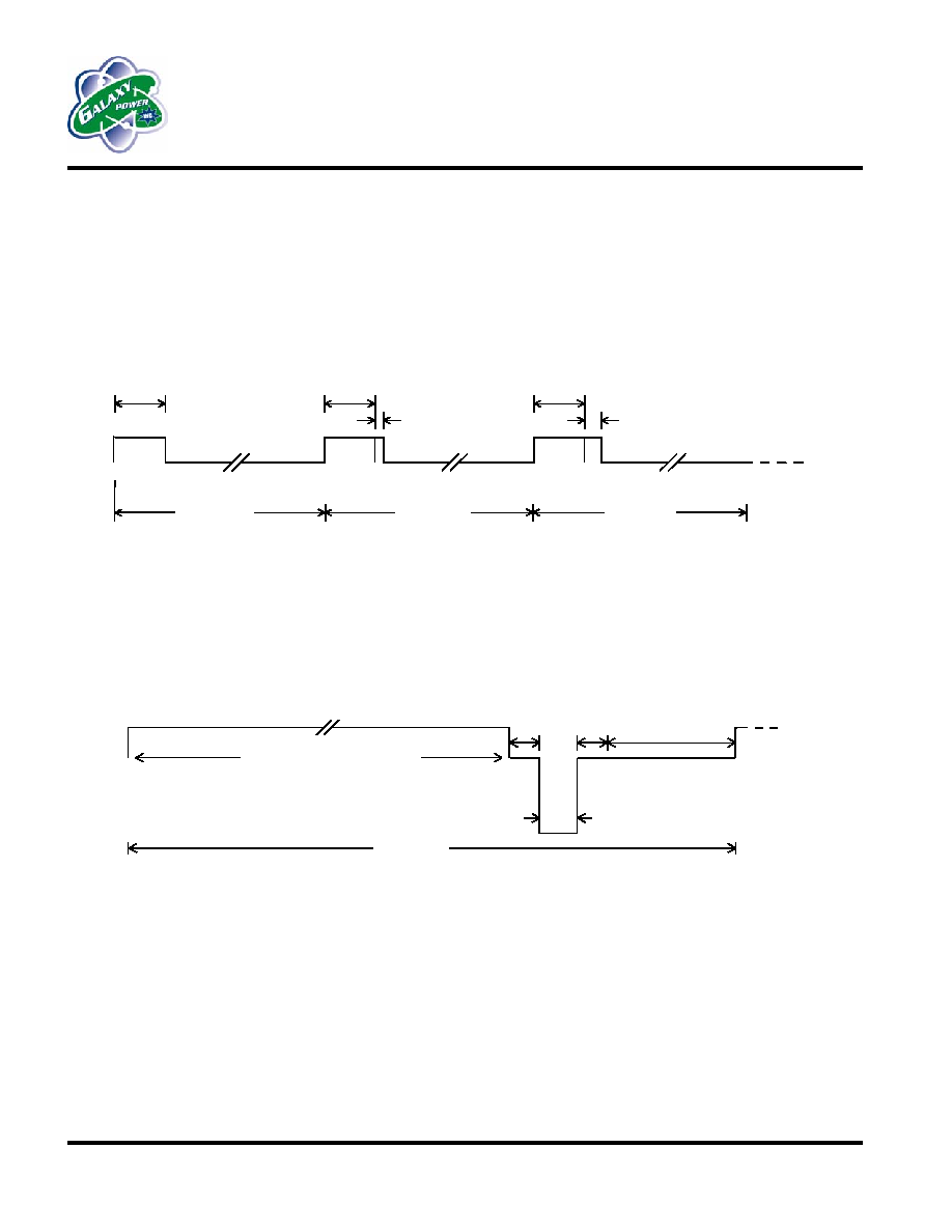
Soft Start Conditioning Charge Duty Cycle
Lithium-ion batteries that have been over-discharged or those taken out of long-term storage do not accept charge readily. To
manage this condition, the ICS1738 applies a 2 minute Soft Start conditioning charge that gradually increases the duty cycle of
the charge, alleviating the battery's reluctance to accept charge. The initial current pulse is approximately 200ms using a 15K
resistor and 100pF capacitor for timing. The duty cycle of the applied current is gradually increased to the fast charge rate, as
shown in Figure 2, by extending the current pulse on every cycle until the pulse is about typically 1.1 seconds in duration. The
CMN indicator is a continuous active low during the Soft Start conditioning stage.
Figure 2: Soft Start Charge Pulse Width Cycle-to-Cycle Increase
Fast Charge Conditioning Duty Cycle
In the second stage, the ICS1738 applies charge in a repetitive sequence consisting of a positive charge pulse followed by a
rest time, an optional discharge pulse, another rest time, ending with a battery voltage acquisition time. The cycle, shown in
Figure 3, repeats every 1.1 seconds using a 15K timing resistor at RC pin 5. The continuous active low CMN indication from
the Soft Start stage continues into and throughout the fast charge stage. Discharge pulse conditioning is not active during the
Soft Start stage, but becomes active at the beginning of the fast charge stage and continues throughout the charge process.
Figure 3: Fast Charge Stage Duty Cycle with Discharge Pulse Conditioning
The amplitude of the charging current pulse is determined by consulting the battery manufacturer's data sheet, taking into
account the charging environment. Parameters such as the current and voltage capability of the charging system and the
required recharge time are two other important considerations. The amplitude of the charge current for lithium-ion batteries is
often set near the 1C ampere-hour rating of the battery. The amplitude of the conditioning discharge current pulse is
determined by consulting the battery data sheet, taking into account the charging environment. The amplitude of the
conditioning discharge current pulse is typically set at about the same amplitude as the charging current limit based on either
4.1V/cell or 4.2V/cell. The discharge pulse width is typically 5ms every 1.1 seconds, so the external transistor and resistor
selected for accomplishing the discharge pulse are determined using conservative pulse ratings. The duty cycle of the reverse
pulse is 0.5% maximum of the fast charge duty cycle. Since the discharge current is rectangular, the RMS current in the resistor
and transistor (logic NFET, high gain NPN, or NPN darlington) is equal to the peak current times the square root of the duty
cycle. So the RMS heating effect current is about 7% of the discharge current peak amplitude. Using conservative pulsed,
rather than steady-state ratings, for selecting the discharge resistor and transistor results in relatively small, low cost devices.
Initial Pulse
Width
cycle time
cycle time
cycle time
Initial Pulse
Width
Initial Pulse
Width
increment
time
2 x increment
time
fast charge pulse width
acquisition time
rest
time
rest
time
discharge pulse width
voltage
cycle time
ICS1738
4
Fast Charge Timer
The ICS1738 has an internal timer limiting the soft-start/fast charge stages to about 3.5 hours using a 15K resistor and 100pF
capacitor at RC pin 5. The timer limit may be decreased proportionally by increasing the resistor value at RC pin 5. For
example to decrease the timer limit by 20% to 2.8 hours, decrease the 15K timing resistor value by 20% to 12K. Similarly to
increase the timer limit by 20% to 4.2 hours, increase the 15K timing resistor value by 20% to 18K. Note that the real time
durations shown in Figure 3 change when the timing resistor at RC pin 5 is changed; however the relative durations within the
cycle always remain proportional to one another. The cycle time with a 15K resistor at RC pin 5 is about 1.1 seconds in fast
charge. The cycle time decreases to about 0.9 seconds if the 12K resistor mentioned in the example above is used. Similarly the
cycle time increases to about 1.32 seconds if the 18K resistor mentioned in the example above is used.
VIN Pin 7 Fast Charge Battery Voltage Data Acquisition and Sensing
In the fast charge stage, a voltage acquisition window occurs after the conditioning discharge current pulse. No charge is
applied during the rest times or during the battery voltage acquisition window. Since no current is flowing while the battery
voltage is measured, the reading is less obscured by surface charge, internal and external voltage changes and noise. If the
discharge pulse option is used, the obscuring effect caused by surface charge is completely removed. ICS1738 VIN pin 7
samples the battery voltage during the voltage acquisition time shown in Figure 3. The latest voltage sample is averaged in
with previous samples, maintaining a record of the battery's voltage through out the fast charge stage. ICS1738 VIN pin 7
senses voltage on two other occasions. Whenever CHG pin 1 goes high, causing the external current source to apply charge to
the battery, the divided down battery voltage at VIN pin 7 is compared to an internal 2V reference during the first 5ms of CHG
pin 1 going high. If the voltage at VIN pin 7 exceeds the internal 2V reference, the ICS1738 shuts down, providing a back-up
over-voltage feature. During the topping and maintenance charge stages mentioned below, the divided down battery voltage at
VIN pin 7 is constantly compared to an internal 0.5V reference. If the voltage at VIN pin 7 drops below the 0.5Vinternal
reference, the ICS1738 shuts down providing a back-up under-voltage feature.
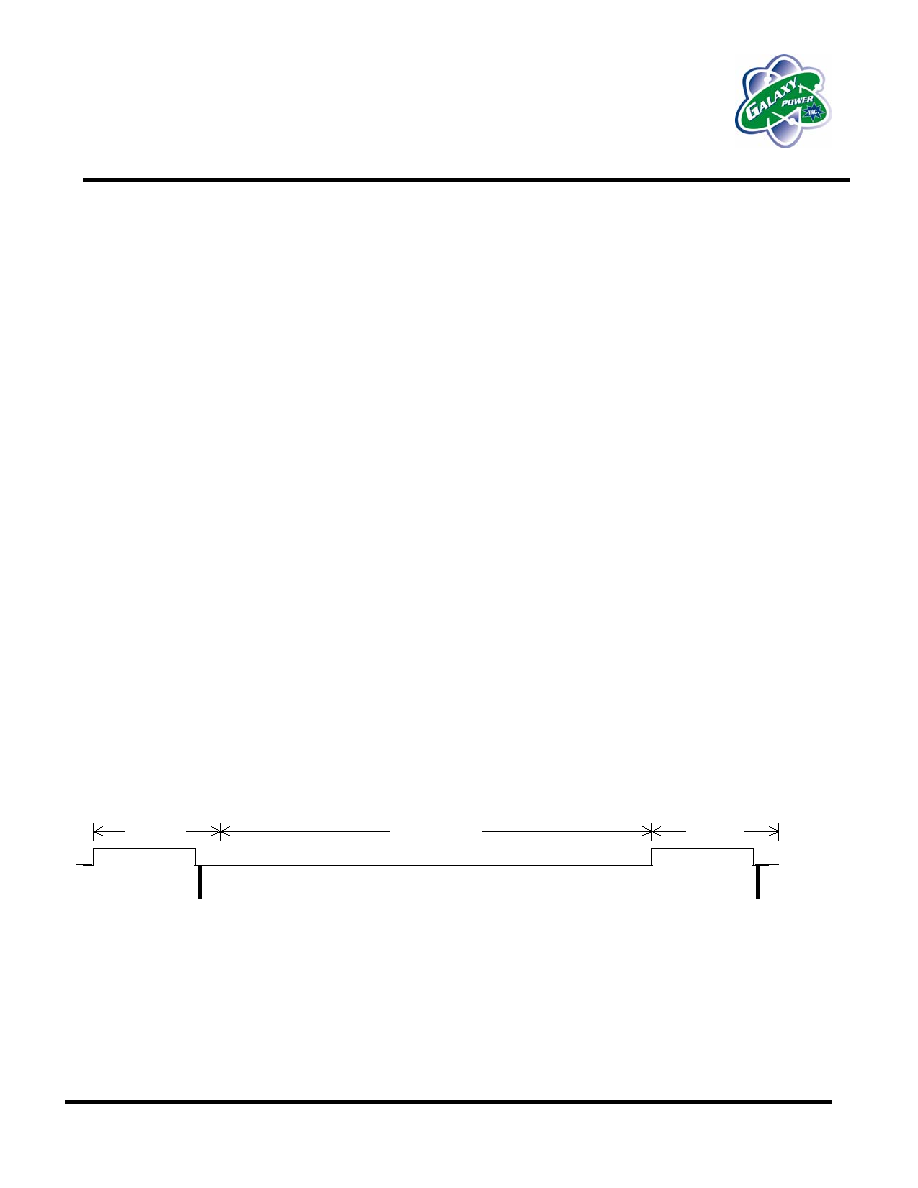
Topping Charge and Maintenance Charge Stages
The third charging stage is a topping charge. The topping charge is not required before putting the battery into immediate
service. The topping charge is an opportunity to add some extra charge without harm compared to constant, unidirectional
voltage charging methods which cause capacity fade, increased series resistance, and increased battery self discharge. The
topping charge is applied for about 2.5 Hours (ref. 15K resistor at RC pin 5). The topping charge consists of the same pulse
technique used during the fast charge stage; however, a delay time is introduced as shown in Figure 4. The delay time between
charge pulses allows the battery to rest, reducing voltage induced stresses in the battery compared to contemporary constant
voltage topping. The same charge pulse that occurs every 1.1 seconds in fast charge rate repeats only once every 5.5 seconds in
the topping stage. A brief conditioning discharge pulse removes voltage-induced stress caused by surface charge on cell
electrodes after every charge pulse. CMN pin 3 indicator goes on (low) and off (open) at a 1Hz rate (ref. 15K timing resistor at
RC pin 5) signaling the battery is ready to use.
CYCLE
DELAY TIME
0 AMP
- DISCHARGE
-----CHARGE
CYCLE
Figure 4: Topping and Maintenance Charge Stage Timing Diagram
The maintenance charge is intended to offset natural battery self-discharge and maintain the battery at peak charge. The
maintenance stage begins after the topping charge stage ends, whereupon the ICS1738 extends the delay time between charge
pulses to 22 seconds with a 15K timing resistor at RC pin 5. A conditioning discharge current pulse follows each charge pulse.
The discharge pulse and delay time between charge pulses reduces voltage-induced stress in the battery reducing capacity fade,
self-discharge, and series resistance build-up compared to constant voltage maintenance charging. CMN pin 3 indicator blinks
at a 1Hz rate (15K timing resistor) as in the topping stage, continuing to signal that the battery is full, ready to use.

5
ICS1738
Fast Charge Termination
Fast Charge Timer Termination
Two methods can be used for terminating fast charge. The simplest, lowest cost charging system using the ICS1738 is the 3.5
hour timed charge in embedded applications that doesn't use the reverse pulse. See the section example in Application
Examples for details on 3.5 Hr embedded and charger stand applications. Embedded applications include those where the
ICS1738 is physically in the battery pack and those where the ICS1738 is in a product along with the battery pack and the
battery pack is not normally removed except for service or repair. So for embedded applications, there is often no need for
external circuits for detecting battery insertion and removal, however note that during evaluations the over/under-voltage
features activate when the battery is disconnected. The fast charge timer is always enabled, however it can be adjusted by
changing the clock frequency as mentioned in section Fast Charge Duty Cycle. Using the ICS1738 3.5 hour fast charge timer
to end charge in both embedded and charger stand application lowers system costs. Charger stand applications that require
battery detection (insertion, removal, or pack protective circuit activation detection) and those that use minimum current
criteria for terminating fast charge along with the reverse pulse conditioning option is more involved since each of these
features requires some external components. See the section Application Examples for detailed information.
Fast Charge Termination Using Minimum Current
A common method for ending fast charge to lithium-ion batteries involves detecting a minimum current amplitude, such as 5%
to 15% of the charging source maximum current set point. The lower the minimum current level, the higher the charge level
and the longer the fast charge time. With the ICS1738, the minimum current level is set externally so that it can be set at any
level desired. Using this method with the ICS1738 involves using the divided down battery voltage used by the charger's
output voltage control. A 3 to 6mV/cell increase to the battery voltage feedback signal is introduced when the charge current
drops to the minimum charge current amplitude chosen to end fast charge. The 3 to 6mV/cell change lowers the end of charge
voltage slightly causing a reduction or temporary elimination of charge current to the battery. The ICS1738 uses a timed-based
weighed data averaging technique to determine when to end fast charge. Average voltage changes prior to and after the 3 to
6mV/cell change are compared to determine when to end fast charge after the minimum current level occurs. This method is
backed-up by the fast charge timer. The timer is always enabled, but can be adjusted by changing the clock frequency as
mentioned previously in the section Fast Charge Timer.
CMN Pin 3 Status Indicator Description List
CMN Charge
Status
1Hz Blink
Charge complete (battery ready to use) as topping/maintenance charges are applied
On
Fast charging (including Soft Start conditioning)
1 Blink
At power-up or with battery insertion, possible back-up over-voltage shut down activation
Off
With input power present: battery removal or shutdown from over/under-voltage back-ups
Charging Stage Duty Cycles
Typical Charge CHG Pin 1 Pulse Duty Cycle (RC = 15K, 100pF)
Fast Charge Pulse
Rate
Topping Charge Pulse
Rate
Maintenance Charge
Pulse Rate
Fast Charge Timer
Duration (after power-
up or battery insertion)
one every 1.1 sec
one every 5.5 seconds
one every 22 seconds
3.5 hr

ICS1738
6
Battery Detection for Charger Stand Applications
When the battery is removable from the product for charging in a stand or when the ICS1738 is in a charger that connects to
the battery, battery or charger insertion and removal is managed using external provisions to briefly override the ICS1738
under/over-voltage shut down features. Switching on and off the input of the 5V supply to the ICS1738 or the 5V to the
ICS1738 is recommended. The simplest, lowest cost automatic approaches involve using a mechanical switch in the battery
well or slot in the stand, or battery connector positions that deliver 5V to the ICS1738 when the battery connects. The battery's
physical presence activates switch contacts that either connects the input supply to the input of the 5V regulator powering
ICS1738 VDD pin 8 or connects the 5V directly to ICS1738 VDD pin 8. See the section Application Examples for detailed
information on automatic electronic methods for managing battery insertion and removal for charger stand applications. Some
Lithium-ion batteries have a third terminal that might assist circuits in applying 5VDC to ICS1738 VDD pin 8 upon battery
insertion and removal. Irrespective of the method used in applying and removing 5VDC to the ICS1738, power-up and down
transitional voltage states should not have plateaus in between 1V and 4.85VDC. For the ICS1738 to shut off completely, its
VDD pin 8 supply must drop below 1V. The resistance between the 5V supply and ICS1738 VDD pin 8 should not exceed 1
.
Battery Voltage Divider Resistor Examples for Setting Charger Voltage Regulator
The ICS1738 comes in two versions: an unmarked version for 4.2V/cell applications and a marked "X" version for 4.1V/cell
applications. The difference between the ICS1738 versions involves the reference level provided by VREF pin 6 and the
approximate 2V internal reference for back-up over-voltage shutdown using VIN pin 7. The reference at pin 6 can be used by
an external op-amp to create the voltage regulator portion of the charging source. Resistor R4A shown in Fig. 6 is used for
ending fast charge using the minimum current method described in the section Fast Charge Termination using Minimum
Current. When the minimum current level occurs, electronic switching circuit (SW) removes R4A from the circuit introducing
a lowering of the voltage limit corresponding to a 3 to 6mV/cell decline in battery voltage. ICS1738 VIN pin 7 samples the
rate at which the battery voltage declines and ends fast charge soon after. The actual time after the electronic switch circuit SW
starts activating and when the ICS1738 ends fast charge is based on the battery's response to the change and the charge level in
the battery prior to the start of recharge. Fast charge termination on an already full battery typically occurs within 4 to 10
minutes from the start of charge. Resistors R3, R4, and R4A in Fig. 6 divide the battery voltage for an op-amp to compare the
battery voltage to ICS1738 VREF pin 6, which is supplied to the other input of the op-amp through R5. R5 is set to the closest
5% standard value resistor based on calculating the parallel combination of R3 and R4 minus 1150 ohms (the typical series
resistance of ICS1738 VREF pin 6). Resistors R3, R4, and R4A (when used) divide the battery voltage so that the charging
source voltage limit nominally occurs at .085V/cell or more below the minimum active over-voltage protection provided in 1
cell lithium-ion battery packs. The .085V/cell difference is increased by at least .008V/cell for 2, 3, and 4 cell packs with R4A
in circuit. R4A increases the charging voltage limit 3 to 6mV/cell higher than R3/R4 divider alone provides without R4A in
circuit. For 4.2V/cell end of charge battery, the minimum active over-voltage protection provided inside the battery pack is
usually set at 4.25V/cell minimum. So for a 1 cell 4.2V end of charge battery, R3 and R4 are based on setting the nominal
charging source voltage limit no higher than 4.165V. For a 2 cell, 8.4Vend of charge battery, R3, R4 and R4A set the nominal
charging source voltage limit to (2 x .085V) + .016V or .186V below the 8.5V minimum pack shutdown resulting in a 8.314V
nominal maximum with R4A in circuit. For a 3 cell, 12.6V end of charge battery, the voltage limit is 12.471V nominal: (3 x
.085V) + (3 x .008V) or .279V below the 12.75V minimum pack shut down. For a 4 cell, 16.8V end of charge battery, the
voltage is limited to 16.628V nominal maximum (.372V below the 17.00V minimum pack shut down), with R4A in circuit.
Figure 6: Divider Resistors for External Op-Amp for ICS1738 4.2V/cell and 4.1V/cell versions
ICS1738 PIN 6 VREF
Type and
# of Li-Ion
cells in
series
SW
+/- 0.5%
R3
+/- 5/10 %
R4A
+/- 0.5%
R4
+/- 5%
R5
Op-Amp for setting charging
source voltage limit. Switch SW
used for min. current termination.
Note: SW and R4A not required for
3.5hr timer termination: See
section Applications Examples

7
ICS1738
The same procedure is used 4.1V/cell end of charge battery packs, based on the over-voltage protection provided inside the
4.1V/cell packs being set at 4.15V/cell minimum. +/- 0.5% resistors are used at their nominal resistance along with the
ICS1738 VREF pin 6 at its nominal value: 1.2944V for the 4.2V/cell version; 1.3206V for the 4.1V/cell "X" version in Tables
6A and 6B. Using this procedure insures that the end of charge voltage stays below the minimum pack over-voltage
protection thresholds as component tolerances vary in a 0
°C to 55 °C environment.
Table 6A: Minimum Current Termination Examples (4.2V/cell Version: VREF = 1.2944V Nominal)
R3/R4 Divider for Low Cost Bipolar Input Op Amp Types
Number of 4.2V/cell Li-
Ion Cells in Series (Max.
Nom. End of Charge)
R3
+/- 0.5%
Tolerance
R4
+/- 0.5%
Tolerance
Actual Nominal Charge
Voltage Limit with
R3, R4, R4A in circuit
R5
+/- 5 %
Tolerance
*R4A: I min
Termination
3 to 6mV/cell
Typ.
+/-5 or 10% tol.
1 (4.165V)
44.2K
20.0K
4.161V
13K
10M
2 (8.314V)
130K
24.0K
8.314V
20K
18M
3 (12.471V)
169K
19.6K
12.470V
16K
15M
4 (16.628V)
232K
19.6K
16.628V
16K
24M
5% Resistor R5 to ICS1738 pin 6 = [(R3 x R4)
÷(R3 + R4)] 1150 Ohms
*R4A and SW are not required for 3.5hr. timer only termination of fast charge
Table 6B: Minimum Current Termination Examples (4.1V/cell "X"Version: VREF = 1.3206V Nominal)
R3/R4 Divider for Low Cost Bipolar Input Op Amp Types
Number of 4.1V/cell Li-
Ion Cells in Series (Max.
Nom. End of Charge)
R3
+/- 0.5%
Tolerance
R4
+/- 0.5%
Tolerance
Actual Nominal
End of Charge
Voltage:
(R4A in circuit)
R5
+/- 5 %
Tolerance
*R4A: I min
Termination
3 to 6mV/cell
Typ.
+/-5 or 10% tol.
1 (4.065V)
44.2K
21.3K
4.065V
13K
13M
2 (8.114V)
129K
25.2K
8.092V
20K
15M
3 (12.171V)
164K
20.0K
12.164V
16K
15M
4 (16.228V)
221K
19.6K
16.227V
16K
18M
5% Resistor R5 to ICS1738 pin 6 = [(R3 x R4)
÷(R3 + R4)] 1150 Ohms
*
R4A and SW are not required for 3.5hr. timer only termination of fast charge
Note: The resistor values in Tables 6A and 6B are for lower cost, single supply, bipolar input op-amps that have
moderate input impedance. For single supply FET input op-amps Table 6 values may be increased by a factor of 10,
except that R4A and SW should change to that shown below to avoid having to use very high value resistors for R4A.
Note that in this configuration SW opens when minimum current occurs. Values shown are for a 4.2V, 1 cell
FET
OP AMP
INPUT
SW
+
4.2V Li-Ion
Battery
+/-5%
R4A
300
+/-0.5%
R4
200K
R3
+/-0.5%
442K

ICS1738
8
VIN
Pin 7
ICS1738
Type and
# of Li-Ion
cells in
series
+
R2
R1
Figure 7: Resistor Divider Network For ICS1738 VIN pin 7 (See Tables 7A, 7B, 8A, 8B)
+/-1% Divider Selection Examples for ICS1738 pin 7 Sensing and Back-up Over-Voltage Shut Down
In addition to VIN pin 7 sampling the change in battery voltage for ending fast charge using the minimum current method
mentioned previously, VIN pin 7 provides back up over-voltage protection. Resistors R1 and R2 shown in Figure 7 divide the
battery voltage to VIN pin 7, setting a back-up over-voltage shutdown to the main over-voltage protection provided inside
lithium-ion battery packs. The divided down battery voltage at VIN pin 7 is compared to an internal 2V reference during the
first 5ms of CHG pin 1 going high. There are two ICS1738 versions: an unmarked version for 4.2V/cell applications and a
marked "X" version for 4.1V/cell applications. The difference in ICS1738 versions also involves the internal 2V reference
used for the back-up over-voltage shutdown. 1% resistors R1 and R2 in Tables 7A and 7B are used to set the over-voltage shut
down of the ICS1738 if the battery voltage or the voltage at the charger terminals rises into the active over-voltage protection
region or above provided in lithium-ion battery packs. For the examples provided in Table 7A for the 4.2V/cell version, the
ICS1738 back-up over-voltage shutdown activates near 4.26V/cell as a minimum, including tolerances (the resistors,at +/-1%,
ICS1738 internal reference at its minimum, etc.). Similarly, examples in Table 7B are for the ICS1738 4.1V/cell version with
its back-up over-voltage shutdown set near 4.14V/cell, as a minimum. As in Tables 6A and 6B, careful attention must be
exercised to insure that resistor value selection does not become a significant source of error in dividing the battery
voltage, however the internal 2Vreference tracks pin 6 reference providing margin for transient conditions.
Table 7A: 1% R1/R2 Divider Resistors for ICS1738 Pin 7 Sensing (4.2V/cell Version)
Back-up Over-Voltage Shut Down Min. Set Near Pack 4.25V Shut Down Min. (VIN pin 7 Shut Down = 1.970V Min.)
# of 4.2V/Cell Li-
Ion cells in series
R1
+/- 1% Tolerance
R2
+/- 1% Tolerance
1 267K
221K
2 681K
200K
3 562K
100K
4 887K
113K
Overall Back-up Shutdown Range: Minimum = 4.26V/cell, Maximum (4 cell) = 4.62V/cell
Table 7B: 1% R1/R2 Divider Resistors for ICS1738 Pin 7 Sensing (4.1V/cell "X" Version)
Back-up Over-Voltage Shut Down Min. Set Near 4.15V Pack Shut Down Min. (VIN pin 7 Shut Down = 2.017V Min.)
# of 4.1V/Cell Li-
Ion cells in series
R1
+/- 1% Tolerance
R2
+/- 1% Tolerance
1 221K
205K
2 634K
200K
3 536K
102K
4 845K
115K
Overall Back-up Shutdown Range: Minimum.= 4.14V/cell, Maximum (4 cell) = 4.46V/cell
9
ICS1738
+/-5% Divider Examples: ICS1738 pin 7 Sensing and Back-up Over-Voltage Shutdown Above Pack Min. Shut Down
The internal back up over-voltage protection feature in the ICS1738 is always active. The battery divider can be selected so
that the ICS1738 back-up over-voltage shutdown occurs only above the active over-voltage range of the Li-Ion battery pack
protector using +/- 5% resistors. For the 4.2V/cell version the values shown in Table 7C raise the ICS1738 back-up over-
voltage shutdown above 4.25V/cell as a minimum using lower cost, +/-5% resistors for cost sensitive applications. For the
4.1V/cell version the values shown below raise the ICS1738 back-up over-voltage shutdown to activate above 4.15V/cell as a
minimum using lower cost, +/-5% resistors for cost sensitive applications. Using +/-5% resistors has no effect on the ICS1738
using the minimum current method for fast charge termination since the 3 to 6mV/cell drop in the charging voltage previously
described is a relative difference.
Table 7C: +/-5
% R1/R2 Divider Resistors for ICS1738 Pin 7 Sensing (4.2V/cell Version)
Back-up Over-Voltage Shut Down Min. Set Above 4.25V Pack Min. Shut Down (VIN pin 7 shut down = 1.970V Min.)
# of 4.2V/Cell Li-
Ion cells in series
R1
+/- 5% Tolerance
R2
+/- 5% Tolerance
1 130K
100K
2 560K
150K
3 910K
150K
4 1.1M
130K
Overall Back-up Shutdown Range: 4.25V/cell Minimum, 5.31V/cell Maximum (4 cell)
Table 7D: +/-5
% R1/R2 Divider Resistors for ICS1738 Pin 7 Sensing (4.1V/cell "X" Version)
Back-up Over-Voltage Shut Down Minimum Set Above 4.15V/cell Pack Min. Shut Down (VIN pin 7 = 2.017V Min.
)
# of 4.1V/Cell Li-
Ion cells in series
R1
+/- 5% Tolerance
R2
+/- 5% Tolerance
1 130K
110K
2 620K
120K
3 750K
130K
4 1.2M
150K
Overall Back-up Shutdown Range: 4.15V/cell Minimum, 5.17V/cell Maximum (4 cell)
Printed Circuit Board and Charging Source Design Considerations
It is important that care be taken to minimize noise coupling and ground bounce. Careful placement of wires and connectors
helps minimize resistance, inductance and coupling between circuits. Charging source on/off transient voltages on the battery
must be low in amplitude. This is especially important when the regulated charging source is a switch mode type. The effects
of line frequency ripple voltage appearing on the battery will interfere with proper performance. When designing the printed
circuit board, make sure ground and power traces are wide and power supply bypass capacitors are located very close to the
IC's supply and ground pins. Use separate, heavy grounds for both signal and power circuits, connecting signal and power
grounds together at one point very close to where the negative lead of the battery connects. For power circuits, keep the
physical separation between power and its return (ground) to a minimum to minimize field effects. Keep the ICS1738 and the
charging source control circuits outside the power and its return loop. Insure that signal lines do not jump across over power
and power return paths. These precautions prevent fields and coupled noise effects from disturbing normal operation especially
when the charging source is a switch mode type.

ICS1738
10
Applications Information
Charge and Use Applications
Charging the battery in products that draw a known and fairly constant current off the battery while the battery is charging
should have this current draw accounted for in the charging source current profile including the minimum current termination
method if used. Using the ICS1738 for charging batteries in products that randomly or periodically require moderate current
from the battery during fast charge needs evaluation. The ICS1738 is not recommended for use in products that randomly or
periodically draw significant current from the battery during fast charge. Charging source conditions that may cause an early
termination of fast charge using the ICS1738 include inadequate input voltage and/or line frequency voltage ripple attenuation.
See the ICS1733 data sheet which describes time based modes that are immune to the above described conditions.
Application Examples
Embedded and charger stand application examples that operate from a regulated input supply are provided. Examples include
low cost 3.5 hour embedded and charger stand implementations as well as full-featured minimum current termination
embedded and charger stand implementations. These circuits may require some adjustments determined by user evaluations.
FETKY or MOSKEY
GND
U2
LM358
6
5
7
8
2
3
4
1
G
S
K
+5VDC
3%
+VIN
1.1A
BAS16
BATT+
+
ICS1738
CHG
DCHG
CMN
VSS
VDD
VIN
VREF
RC
U1
+
100uF
LED
+
.01uF
BATT-
.01uF
100pF
.01uF
BAS16
4.7K
.5W
.20
390
390
R1
130K
R2
100K
.5%
R3
44.2K
.5%
R4
20.0K
15K
R5
13K
1%
19.6K
1%
49.9K
1%
22.6K
1%
49.9K
Figure 8A: Low Cost 3.5 Hour Embedded Application Example (4.2V Single Cell Version)
Note: Battery pack has active/ passive current, voltage, and thermal protection required by the cell's manufacturer

11
ICS1738
Table 8A: Low Cost 3.5 Hour Embedded Application Example (4.2V Single Cell Version)
#
Comp.
Des.
Pkg.
Type
Component Information and Operational Details
Note: Refer to Figure 8A. This low cost application is a specific 1 cell embedded example where fast charge
termination is the ICS1738 3.5 hour timer. Inputs other than 5V +/-3% require modification to
this approach. If applicable refer to the section Applications Information Charge and Use Applications.
This circuit may require some adjustments determined by user evaluations.
1
LED
2 Pin
ICS1738 pin 3 CMN connects LED cathode to ground continuously turning ON LED to indicate fast charge.
ICS1738 pin 3 CMN blinks LED about once every second to indicate charge complete while topping and
maintenance charge are applied
2
U2
R3,R4
8 Pin
U2 LM358 is a low cost, dual, single-supply op-amp. U2 input pin 3 senses the input side of .20 Ohm current sense
resistor via 22.6K/49.9K 1% divider providing 3.44V typical which is below pin 3 maximum common mode sensing
limit (5V-1.5V = 3.5V). U2 pin 2 senses the other side of the.20 Ohm current sense resistor via 19.6K/49.9K 1%
divider. U2 pin 1 controls a FETKY device made by International Rectifier IRF7534D1 (8 pin SOIC) or by On
Semiconductor NTMSD2P102LR2 (8 pin SOIC) or a MOSKEY device made by Microsemi Corporation
UDFS320P (3 pin surface mount) .20V is dropped across .20 Ohm provided a 1Amp current limit. U2 pin 6 senses
the divided down battery voltage via R3/R4 44.2K/20.0K 0.5% divider with U2 pin 5 connected to U1 ICS1738 pin
6 reference. See Table 6B for values for R3 and R4 for 4.1V single cell version. U2 pin 7 regulates the charge
voltage by pulling down on U2 pin 2 via BAS16, a low cost SOT23 diode made by Fairchild Semiconductor and
Diodes, Inc. Other signal type diodes may be used. When ICS1738 pin 1 CHG goes high (to 5V) it allows U2 pin 1
to go low switching on the FETKY or MOSKEY, applying charge to the battery. U2 pin 2controls the charge
voltage by adjusting the turn on of the FETKY or MOSKEY as the battery voltage approaches the limit. A .01 uF
capacitor between U2 pin 1 and U2 pin 2 provides feedback compensation for stable regulation. When ICS1738 pin
1 CHG goes low (to 0V), U2 pin 1 output is high, so the FETKY or MOSKEY remains off and no charge is applied
to the battery.
3
R1,R2
130K/100K values shown raise the ICS1738 back-up over-voltage shutdown above 4.25V/cell as a minimum using
low cost, +/-5% resistors for cost sensitive applications. See Table 7A for 1% values. See Table 7B and 7D for
values for R3 and R4 for 4.1V single cell version. If the back-up over-voltage is activated, U1 ICS1738 shuts down
and does not restart unless input power (+V) is removed and the fault condition is corrected. Then the ICS1738
restarts when input power (+V) is reapplied.
4
R5
R5 13K is the closest 5% standard value resistor based on calculating the parallel combination of R3 and R4 minus
1150 ohms (the typical series resistance of ICS1738 VREF pin 6).
5
100uF
.01uF
Filter capacitors are used for noise suppression and stability in this linear application. Typically an additional .1uF
per mA for power and an additional .01uF per mA for control devices should be adequate for this linear application.
6 15K
100pF
Sets
U1
ICS1738 timing at 1MHz typical.

ICS1738
12
Figure 8B: Low Cost 3.5 Hour Charger Stand Application Example (4.2V Single Cell Version)
BAS16
XN04601
BATT-
BATT+
S
K
G
REG. INPUT
1
4
2
3
8
5
6
7
C
B
E
4
3
2
5
1
.1W
6
5V
6V
ECJRVFIE1042
.1uF
+
LM358
U2
AN1431
VR1
1.2A
6V
ICS1738
CHG
DCHG
CMN
VSS
VDD
VIN
VREF
RC
U1
FETKY or MOSKEY
390
EXS8V391J
+
100 uF
100pF
+
.01uF
.01uF
LED
4.7K
4.7K
UNR221L
4.7K
.25 W
10
1%
1K
1%
1K
R1
130K
R2 100K
15K
R5
13K
.5%
R3
44.2K
.5%
R4
20.0K
2W
.75
220
390
680K
1.6M
270K
110K
1.6M
Note: Battery pack has active/ passive current, voltage, and thermal protection required by the cell's manufacturer

13
ICS1738
Table 8B: Low Cost 3.5 Hour Charger Stand Application Example (4.2V Single Cell Version)
#
Comp.
Des.
Pkg.
Type
Component Information and Operational Details
Note: Refer to Figure 8B. This low cost application is a specific 1 cell charger stand example where fast charge
termination uses the ICS1738 3.5 hour timer. Inputs other than regulated 6V will require component
value changes. This circuit may require some adjustments determined by user evaluations.
1
LED
2 Pin
ICS1738 pin 3 CMN connects LED cathode to ground continuously turning ON LED to indicate fast charge. ICS1738
pin 3 CMN blinks LED about once every second to indicate charge complete while topping and maintenance charge
are applied.
2
U2
UNR221L
8 Pin
3 Pin
U2 LM358 is a low cost, dual, single supply bipolar op-amp. U2 input pin 3 senses a voltage pulse from a 270K
resistor and a .1uF capacitor in parallel with it that connected to BATT+. The .1uF capacitor is in network (Panasonic
ECJRVF1042). The pulse is initiated by U1 ICS1738 pin 1 CHG going high for a few milliseconds every second when
the battery is missing. U2 pin 3 has a voltage reference on it produced by a 1.6M pull-up to +V (6.0V) and a 680K pull-
up to U1 ICS1738 pin 6 reference. U2 output pin 1 switches UNR221L (Panasonic) off and a 390 Ohm resistor in a
Panasonic EXS8V391J resistor network insures the +5V supplying U1 ICS1738 goes low (below 1V) for several ms
every second until the battery connects. A .1uF capacitor and 1.6M resistor provide feedback from U2 pin 1 to U2 pin
3. On Semiconductor makes a MUN5132T1 that is similar to UNR221L. ROHM, Co. LTD also makes a similar
device as well as low cost resistor networks.
3
U2, R3,
R4
U2 LM358 op-amp input pin 6 compares divided down battery voltage via R3/R4 44.2K/20.0K 0.5% to the reference
voltage on its input pin 5 provided by U1 ICS1738 pin 6 via R5, a 12K resistor. 12K is the closest 5% standard value
resistor based on calculating the parallel combination of R3 and R4 minus 1150 ohms (the typical series resistance of
ICS1738 VREF pin 6). U2 pin 7 output adjusts the PNP transistor in XN04601 (Panasonic) controlling a FETKY
device made by International Rectifier IRF7534D1 (8 pin SOIC) or by On Semiconductor NTMSD2P102LR2 (8 pin
SOIC). A MOSKEY device made by Microsemi Corporation UDFS320P (3 pin surface mount) can also be used. .01uF
between U2 pin 7 and U2 pin 6 provides feedback compensation for stable regulation. The base emitter of the PNP
transistor in XN04601 provides a 1Amp maximum current limit unless U2 pin 7 output pulls down on its base causing
it to adjust the drop across the FETKY (or MOSKEY) device to regulate the charger output voltage.
3
R1,R2
130K/100K values shown raise the ICS1738 back-up over-voltage shutdown above 4.25V/cell as a minimum using
low cost, +/-5% resistors for cost sensitive applications. See Table 7A for 1% values. See Table 7B and 7D for values
for R3 and R4 for 4.1V single cell version. If the back-up over-voltage is activated, U1 ICS1738 shuts down and does
not restart until the input power (+V) is removed, the fault condition is corrected, and input is reapplied.
4
XN04601
6 Pin
The NPN transistor in XN04601 is used by U1 ICS1738 pin 1 to turn on and off the FETKY (MOSKEY) device
providing charge on/off. ROHM, Co. LTD also makes a device similar to the XN04601.
5
BAS16
3 Pin
BAS16 SOT-23 diode made by Fairchild Semiconductor and Diodes, Inc. connects from U1 ICS1738 pin 6 to pin 7
keeping pin 7 above 0.5V so the ICS1738 internal under-voltage shutdown does not activate when the charged battery
is disconnected. Other signal diode types may be used for this purpose.
6
VR1
3 Pin
VR1, AN1431 made by Panasonic (or LM431 made by several other manufacturers) is a 2.5V shunt regulator that
provides a low cost, low drop out 5V +/- 3% for powering U1 ICS1738. Two 1K 1% resistors divide the output
(collector) of UNR221L (Panasonic) by two for VR1 comparison to its internal 2.5V reference. A 10 ohm resistor
drops voltage as VR1 shunts current to ground regulating 5V to U1 ICS1738.
7
15K
100pF
Sets
U1
ICS1738 timing at 1MHz typical.
8
100uF,
.1uF
Filter capacitors are used for noise suppression and stability in this linear application. Typically an additional .1uF per
mA for power and an additional .01uF per mA for control devices should be adequate for this linear application.

ICS1738
14
Figure 8C: Full Featured Embedded Application Example (4.2V Single Cell Version)
.
1W
1
5
2
3
4
E
B
C
7
6
5
8
3
2
4
1
REG. INPUT
G
K
S
BATT+
BATT-
LED
BAS16
.01uF
.01uF
+
BAS16
100pF
2SD2185
.1uF
+
100 uF
390
EXS8V391J
FETKY or MOSKEY
ICS1738
CHG
DCHG
CMN
VSS
VDD
VIN
VREF
RC
U1
1.2A
6V
AN1431
VR1
XN01401
+
LM358
U2
4.7K
4.7K
UNR521L
18K
220
2W
.75
.5%
R4
20.0K
.5%%
R3
44.2K
R5
13K
R4A
10M
15K
1%
R2 200K
1%
R1
237K
.125W
4.3
1%
1k
1%
1k
.25 W
10
4.7K
Note: Battery pack has active/ passive current, voltage, and thermal protection required by the cell's manufacturer

15
ICS1738
#
Comp.
Des.
Pkg.
Type
Table 8C: Full Featured Embedded Application Example (4.2V Single Cell Version)
Component Information and Operational Details
Note: Refer to Figure 8C. This full featured application is a specific 1 cell embedded example where fast charge
termination is the minimum current method using the ICS1738 with discharge pulse conditioning. Inputs other
than regulated 6V may require component value changes. If applicable refer to the Applications Information
Charge and Use Applications. This circuit may require some adjustments determined by user evaluations.
1
2SD2185
3 Pin
Low cost, high gain Panasonic NPN transistor (or similar device) connects a 4.3 Ohm resistor providing
conditioning discharge current pulses after soft start completes.
2 LED
2
Pin ICS1738 pin 3 CMN connects LED cathode to ground continuously turning ON LED to indicate fast charge.
ICS1738 pin 3 CMN blinks LED about once every second to indicate charge complete while topping and
maintenance charge are applied
3 U2
XN01401
R3,R4
8 Pin
5 pin
U2 LM358 is a dual, low cost bipolar op-amp. U2 input pin 3 receives a 2.5V reference from two 1K 1% resistors
that divide down the 5V produced by VR1 as explained below. U2 input pin 2 receives a high signal (5V) from U1
ICS1738 pin 1 for turning on a FETKY or MOSKEY device via a 390 Ohm resistor in a Panasonic EXS8V391J
network. The FETKY or MOSKEY device delivers charge to the battery as allowed by the PNP transistor in
XN01401 (Panasonic) and U2 pin 7. When U2 pin 2 receives a low signal (0V) from U1 ICS1738 pin 1, it switches
off the FETKY or MOSKEY device by going high. A FETKY device is made by International Rectifier IRF7534D1
(8 pin SOIC) or by On Semiconductor NTMSD2P102LR2 (8 pin SOIC) or a MOSKEY device made by Microsemi
Corporation part number UDFS320P (3 pin surface mount) may be used. U2 pin 6 senses divided down battery
voltage via R3/R4 44.2K/20.0K 0.5% divider with U2 pin 5 connected to U1 ICS1738 pin 6 reference. See Table 6B
for values for R3 and R4 for 4.1V single cell version. .01uF between U2 pin 7 and U2 pin 6 provides feedback
compensation for stable regulation. The base emitter of the PNP transistor in the XN01401 (Panasonic) device
provides a 1Amp maximum current limit due to the .75V maximum drop across .75 Ohm 2W resistor. Current limit
only occurs as U2 pin 7 allows since U2 pin 7 pulls down the base of the upper PNP transistor causing the PNP to
adjust the drop across the FETKY (or MOSKEY) device to regulate the charger output voltage. ROHM, Co. Ltd.
also makes a device similar to the XN01401, as well as low cost resistor networks.
4 BAS16
UNR521L
3 Pin
3 Pin
With about 45mA current flow set by an 18K resistor from a BAS16 diode cathode to ground, a 0.56V typical
reference is provided at the base of the lower PNP transistor in the XN01401 (Panasonic) device. As the voltage
across the .75 Ohm 2W current sense resistor drops to about .04V, with about 53mA flowing into the battery, the
lower PNP transistor in the XN01401 (Panasonic) device turns off, causing the UNR521L (Panasonic) device to
shutoff, disconnecting resistor R4A 10M resistor (see Table 6A). Charge current is reduced as R4A is disconnected
and the battery voltage drops several mV/cell. U1 ICS1738 pin 7 detects the change and ends fast charge according
to the batteries response to the change. Then U1 ICS1738 pin 3 blinks DS1 for charge complete (battery ready) and
uses a BAS16 diode (as an option) to turn on the UNR521L (Panasonic) device again so that charge current returns
to the about pre-termination level as the topping charge is applied. On Semiconductor makes a MUN5132T1 that is
similar to UNR521L. ROHM, Co. LTD also makes a similar device, as well as low cost resistor networks.
5 R1,R2
237K/200K 1% resistors from Table 7A raise the ICS1738 back-up over-voltage shutdown near 4.26V/cell as a
minimum. See Table 7C for lower cost, 5% values. See Table 7B and 7D for values for R3 and R4 for 4.1V single
cell version. If the back-up over-voltage is activated U1 ICS1738 shuts down and does not restart until the fault
condition is corrected and input power (+V) is removed and reapplied.
6 15K
100pF
Sets
U1
ICS1738 timing at 1MHz typical.
7 VR1
3 Pin
VR1, AN1431 made by Panasonic (or LM431 made by several other manufacturers), 2.5V shunt regulator provides
a low cost, low drop out 5V +/- 3% for powering U1 ICS1738. Two 1K 1% resistors divide VR1 cathode for
comparison to VR1 internal 2.5V reference. A 10 ohm resistor drops voltage as VR1 shunts current to ground
regulating 5V to U1 ICS1738.

ICS1738
16
BAS16
GND
4
OUT 2
CONT 5
IN
1
BATT-
BATT+
S
K
G
REG. INPUT
1
4
2
3
8
5
6
7
C
B
E
4
3
2
5
1
.
1W
AN80L
50RMS
+5V
.1uF
+
C7
1uF
.01uF
LED
BAS16
.01uF
.01uF
+
BAS16
100pF
2SD2185
.1uF
+
100 uF
390
EXS8V391J
FETKY or MOSKEY
ICS1738
CHG
DCHG
CMN
VSS
VDD
VIN
VREF
RC
U1
1.2A
6V
XN01401
+
LM358
U2
4.7K
4.7K
UNR521L
U6
4.7K
18K
220
2W
.75
.5%
R4
20.0K
.5%%
R3
44.2K
R5
13K
R4A
10M
15K
1%
R2 200K
1%
R1
237K
.125W
4.3
1%
15k
1%
15k
4.7K
Figure 8D: Full Featured Charger Stand Application Example (4.2V Single Cell Version)
Note: Battery pack has active/ passive current, voltage, and thermal protection required by the cell's manufacturer

17
ICS1738
#
Comp.
Des.
Pkg.
Type
Table 8D: Full Featured Charger Application Example (4.2V Single Cell Version)
Component Information and Operational Details
Note: Refer to Figure 8D. This full featured application is a specific 1 cell charger stand example where fast charge
termination is the minimum current method using the ICS1738 with discharge pulse conditioning. Inputs
other than regulated 6V may require component value changes. This charger stand example uses a different
type of battery detection technique compared to the example shown in Figure 8B. This circuit may require
some adjustments determined by user evaluations.
1
2SD2185
3 Pin
Low cost, high gain Panasonic NPN transistor (or similar device) connects a 4.3 Ohm resistor providing
conditioning discharge current pulses after soft start completes.
2 LED
2 Pin
See previous examples
3 U2
XN01401
R3,R4
8 Pin
5 pin
U2 LM358 is a dual, low cost bipolar op-amp. U2 input pin 3 receives a 2.5V reference from two15K resistors that
divide down 5V produced by VR1. U2 input pin 2 receives a high signal (5V) from U1 ICS1738 pin 1 causing U2
pin 1 to switch on a FETKY or MOSKEY device via a 390 Ohm resistor in a Panasonic EXS8V391J resistor
network. The FETKY or MOSKEY device delivers charge to the battery as allowed by the upper PNP transistor in
XN01401 (Panasonic) and by U2 pin 7. When U2 pin 2 receives a low signal (0V) from U1 ICS1738 pin 1, U2 pin 1
output goes high and turns off the FETKY or MOSKEY device. A FETKY device is made by International Rectifier
IRF7534D1 (8 pin SOIC) or by On Semiconductor NTMSD2P102LR2 (8 pin SOIC) or a MOSKEY device made by
Microsemi Corporation part number UDFS320P (3 pin surface mount) may be used. U2 pin 6 senses divided down
battery voltage via R3/R4 44.2K/20.0K 0.5% divider with U2 pin 5 connected to U1 ICS1738 pin 6 reference. See
Table 6B for values for R3 and R4 for 4.1V single cell version. .01uF between U2 pin 7 and U2 pin 6 provides
feedback compensation for stable voltage regulation. The base emitter of the upper PNP transistor in the XN01401
(Panasonic) device provides a 1Amp maximum current limit due to the .75V maximum drop across .75 Ohm, 2W
resistor. Current limit only occurs as U2 pin 7 allows since U2 pin 7 output pulls down on the base of the upper PNP
in the XN01401 causing the PNP to adjust the drop across the FETKY (or MOSKEY) device to regulate the charger
output voltage. ROHM, Co. Ltd. also makes a device similar to the XN01401, as well as low cost resistor networks.
4 BAS16
UNR521L
3 Pin
3 Pin
With about 0.3 mA current flow set by an 18K resistor from a BAS16 diode cathode to ground, a 0.56V typical
reference is provided at the base of the lower PNP transistor in the XN01401 (Panasonic) device. As the voltage
across the .75 Ohm 2W current sense resistor drops to about .04V, with about 53mA into the battery, the lower PNP
transistor in the XN01401 (Panasonic) device turns off, causing the UNR521L (Panasonic) device to shutoff,
disconnecting resistor R4A 5.6M resistor listed in Table 6A. Charge current is reduced as R4A is disconnected and
the battery voltage drops several mV/cell. U1 ICS1738 pin 7 detects the several mV drop in battery voltage and ends
fast charge according to the battery's response to the change. Then U1 ICS1738 pin 3 blinks DS1 for charge
complete (battery ready) and uses a BAS16 diode (as an option) to turn on the UNR521L (Panasonic) device again
so that charge current returns to the about pre-termination level during the topping charge. On Semiconductor makes
a MUN5132T1 a device similar to the Panasonic UNR521L. ROHM, Co. LTD also makes a similar device.
5 R1,R2
237K/200K 1% resistors from Table 7A raise the ICS1738 back-up over-voltage shutdown near 4.26V/cell as a
minimum. See Table 7C for lower cost, 5% values. See Table 7B and 7D for values for R3 and R4 for 4.1V single
cell version. If the back-up over-voltage is activated in U1 ICS1738, it shuts down and does not restart unless the
fault condition is corrected and input power (+V) is reapplied.
6 15K
100pF
Sets
U1
ICS1738 timing at 1MHz typical.
7 VR1
5 or 6
Pin
VR1 low drop regulator (AN80L50RMS is Panasonic) outputs 5V +/- 3% to U1 ICS1738. VR1 turns on as its
CONT pin 5 is raised to a logic high when the battery connects. Devices similar to N80L50RMS include JRC, Ltd.
NJM2370X05, On Semi. MC33263NW-50R2 and its equivalent TOKO Inc. TK11250BMCL. These three devices
have a pin that uses a noise bypass capacitor. The AN80L50RMS does not use a specific pin for noise bypass.

ICS1738
18
Table 9: Absolute Maximums
Voltage to VDD
6.5
V
Input and output pins
-0.5 to VDD
+ 0.5
V
Ambient Operating Temperature
70
°C
Storage Temperature
-55 to 150
°C
Stresses beyond those listed in Table 9 Absolute Maximums may cause permanent damage to the device. This is a stress rating
only. Functional operation of the device at the Absolute Maximum Ratings or other conditions not consistent with the
characteristics stated in this document is not intended. Exposure to absolute maximum conditions also adversely affects
performance.
Table 10: DC Characteristics
T
amb
= 25°C, unless otherwise specified
Parameter Sym
bol
Conditions MIN
TYP
MAX
UNITS
Supply Voltage
V
DD
4.85
5.00
5.15
V
Supply Current
I
DD
7.3
mA
V
DD
= 5.00V
1.2944
V +/- 1.0 %
VREF
4.2V (unmarked version)
V
REF
V
DD
= 5V+/- 3%, T
amb
= 0 to 55°C
1.2944
V +/- 1.4 %
V
DD
= 5.00V
2.0100
V +/- 1.4 %
Over-voltage shutdown
4.2V (unmarked version)
V
IN
V
DD
= 5V+/- 3%, T
amb
= 0 to 55°C
2.0100
V +/- 2%
V
DD
= 5.00V
1.3206
V +/- 1.0 %
VREF
4.1V (marked version)
V
REF
V
DD
= 5V+/- 3%, T
amb
= 0 to 55°C
1.3206
V +/- 1.4 %
V
DD
= 5.00V
2.0582
V +/- 1.4 %
Over-voltage shutdown
4.1V (unmarked version)
V
IN
V
DD
= 5V+/- 3%, T
amb
= 0 to 55°C
2.0582
V +/- 2 %
VREF Series Resistance
V
REF
V
DD
= 5.00V
1150
Ohms
High Level Source CHG
I
OH
V=
V
DD
- 0.4V
25
mA (max)
Low Level Sink CHG
I
OL
V=0.4V
25
mA
(max)
Low Level Sink CMN
I
OL
V=0.4V
40
mA
(max)
Analog/Digital Converter
V
IN
0-2.3
V
19
ICS1738
Table 11: Timing Characteristics
R=15K , C=100pF
PARAMETER PIN
NUMBER
REFERENCE
TYP
UNITS
Clock Frequency
RC Pin 5
1.0
MHz
Conditioning Discharge Pulse Width
DCHG Pin 2
see Figure 3.0
5
ms
Charge Pulse Width in Fast Charge Stage
CHG Pin 1
see Figure 3.0
1048
ms
Rest Times
CHG Pin 1
see Figure 3.0
4.0
ms
Data Acquisition Time
CHG Pin 1
see Figure 3.0
16.4
ms
Cycle Time
CHG Pin 1
see Figure 3.0
1077
ms
Soft Start Initial Pulse Width
CHG Pin 1
see Figure 2.0
200
ms
Soft Start Incremental Pulse Width
CHG Pin 1
see Figure 2.0
7.0
ms
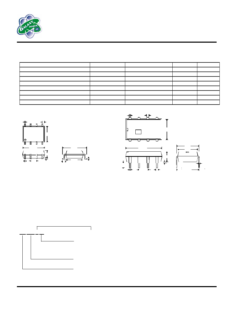
Package Information
Ordering Information
ICS1738S, ICS1738ST, ICS1738N (Package unmarked for 4.2V/cell applications)
ICS1738XS, ICS1738XST, ICS1738XN (X = Package has a mark for 4.1V/cell applications)
Example:
ICS 1738 X ST Version : X = Package has a mark 4.1V/cell , Package unmarked: 4.2V/cell version
Package
type: N=
DIP 300 mil (Plastic)
S=
SOIC
150
mil
ST=
SOIC 150 mil Tape and Reel
Device type:
Consists of 3 to 5 numbers
Prefix:
ICS
=
I
ntelligent
C
harging
S
olution standard device
0 .0 25
0 .0 50
0 .0 0 8
0.23 6
0.15 4
All pa c k ag e d ime n s ion s a re in
in c h es .
0.15 5
0.01 6
0.01 6
0 .0 50
0 .0 0 6
0 .0 5 8
0 .1 9 3
0 .0 0 8
IC S1 7 3 8S
8-Pin SOIC Packag e (150 mil)
0 .0 35
YR W K
GPI
0.018
0.060
0.250
0.375
0.130
0.130
0.015
0.018
0.100
0.060
0.310
0.250
0.350
0.010
All package dimensions are in inches.
8-Pin DIP package (300 mil)
QuickSaver
ICS1738N

ICS1738
20
IMPORTANT NOTICE
Galaxy Power Incorporated makes no claim about the capability of any particular battery in accepting a fast charge. GPI
strongly recommends that the battery manufacturer be consulted before fast charging. GPI shall be held harmless for any
misapplication of this device such as: exceeding the rated specifications of the battery manufacturer; charging batteries other
than rechargeable lithium-ion types; personal or product damage caused by the charging device, circuit, or system itself; unsafe
use, application, and/or manufacture of a charging system using this device.
GPI reserves the right to make changes in the device data identified in this publication without further notice. GPI advises its
customers to obtain the latest version of all device data to verify that any information being relied upon by the customer is
current and accurate.
GPI does not assume any liability arising out of or associated with the application or use of any product or integrated circuit or
component described herein. GPI does not convey any license under its patent rights or the patent rights of others described
herein. In the absence of a written or prior stated agreement to the contrary, the terms and conditions stated on the back of the
GPI order acknowledgment obtain.
GPI makes no warranty of any kind with regard to this material, including, but not limited to, the implied warranties of
merchantability and fitness for a particular purpose.
GPI products are not designed, intended, or authorized for use as components in systems intended for surgical implant into the
body, or other applications intended to support or sustain life, or for any nuclear facility application, or for any other
application in which the failure of the GPI product(s) could create a situation where personal injury or death may occur. GPI
will not knowingly sell its products for use in such applications, and the buyer shall indemnify and hold harmless GPI and its
officers, employees, subsidiaries, affiliates, representatives and distributors against all claims, costs, damages, expenses, tort
and attorney fees arising out of directly or indirectly, any claim of personal injury or death associated with such unintended or
unauthorized use, even if such claim alleges that GPI was negligent regarding the design or manufacture of the part.
COPYRIGHT © 2001 Galaxy Power Incorporated
Galaxy Power, Inc.
PO Box 890
2500 Eisenhower Avenue
Valley Forge, PA 19482-0890
Phone: 610-676-0188
FAX: 610-676-0189
Web: www.galaxypower.com
E-mail:
whitmer@galaxypower.com
REV0 072301