DS07-13737-2E
FUJITSU SEMICONDUCTOR
DATA SHEET
16-bit Proprietary Microcontroller
CMOS
F
2
MC-16LX MB90350 Series
MB90F352/S, MB90352/S
s
s
s
s
DESCRIPTION
The MB90350-series with 1 channel FULL-CAN* interface and FLASH ROM is especially designed for automotive
and industrial applications. Its main feature is the on-board CAN Interface, which conform to V2.0 Part A and Part
B, while supporting a very flexible message buffer scheme and so offering more functions than a normal full CAN
approach. With the new 0.35
µ
m CMOS technology, Fujitsu now offers on-chip FLASH-ROM program memory
up to 128 Kbytes. An internal voltage booster removes the necessity for a second programming voltage.
An on board voltage regulator provides 3 V to the internal MCU core. This creates a major advantage in terms
of EMI and power consumption.
The internal PLL clock frequency multiplier provides an internal 42 ns instruction cycle time from an external
4 MHz clock.
The unit features a 4 channel Output Compare Unit and 6 channel Input Capture Unit with 2 separate 16-bit free
running timers. 2 channels UART constitute additional functionality for communication purposes.
* : Controller Area Network (CAN) - License of Robert Bosch GmbH
Note : F
2
MC stands for FUJITSU Flexible Microcontroller, a registered trademark of FUJITSU LIMITED.
s
s
s
s
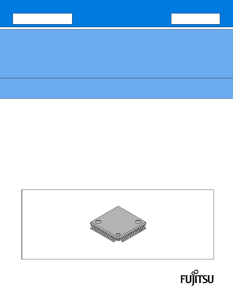
PACKAGE
64-pin Plastic LQFP
(FPT-64P-M09)

MB90350 Series
2
s
s
s
s
FEATURES
·
·
·
·
Clock
· Built-in PLL clock frequency multiplication circuit
· Selection of machine clocks (PLL clocks) is allowed among frequency division by two on oscillation clock, and
multiplication of 1 to 6 times of oscillation clock (for 4 MHz oscillation clock, 4 MHz to 24 MHz).
· Operation by sub-clock (up to 50 kHz : 100 kHz oscillation clock divided by two) is allowed. (devices without
S-suffix only)
· Minimum execution time of instruction : 42 ns (when operating with 4-MHz oscillation clock, and 6-time multi-
plied PLL clock).
· Built-in clock modulation circuit
·
·
·
·
16 Mbyte CPU memory space
· 24-bit internal addressing
·
·
·
·
External Bus Interface
· 4 MByte external memory space
·
·
·
·
Instruction system best suited to controller
· Wide choice of data types (bit, byte, word, and long word)
· Wide choice of addressing modes (23 types)
· Enhanced multiply-divide instructions and RETI instructions
· Enhanced high-precision computing with 32-bit accumulator
·
·
·
·
Instruction system compatible with high-level language (C language) and multitask
· Employing system stack pointer
· Enhanced various pointer indirect instructions
· Barrel shift instructions
·
·
·
·
Increased processing speed
· 4-byte instruction queue
·
·
·
·
Powerful interrupt function
· Powerful 8-level, 34-condition interrupt feature
· Up to 8 channels external interrupts are supported
·
·
·
·
Automatic data transfer function independent of CPU
· Extended intelligent I/O service function (EI
2
OS) : up to 16 channels
· DMA : up to 16 channels
·
·
·
·
Low power consumption (standby) mode
· Sleep mode (a mode that halts CPU operating clock)
· Main timer mode (a timebase timer mode switched from the main clock mode)
· PLL timer mode (a timebase timer mode switched from the PLL clock mode)
· Watch mode (a mode that operates sub clock and clock timer only)
· Stop mode (a mode that stops oscillation clock and sub clock)
· CPU blocking operation mode
·
·
·
·
Process
· CMOS technology
·
·
·
·
I/O port
· General-purpose input/output port (CMOS output)
- 49 ports (devices without S-suffix)
- 51 ports (devices with S-suffix)
(Continued)

MB90350 Series
3
(Continued)
·
·
·
·
Timer
· Time-base timer, clock timer, watchdog timer : 1 channel
· 8/16-bit PPG timer : 8-bit
×
10 channels, or 16-bit
×
6 channels
· 16-bit reload timer : 4 channels
· 16- bit input/output timer
- 16-bit free run timer : 2 channels (FRT0 : ICU0/1, FRT1 : ICU 4/5/6/7, OCU 4/5/6/7)
- 16- bit input capture: (ICU) : 6 channels
- 16-bit output compare : (OCU) : 4 channels
·
·
·
·
Full-CAN interface : 1 channel
· Compliant with Ver2.0A and Ver2.0B CAN specifications
· Flexible message buffering (mailbox and FIFO buffering can be mixed)
· CAN wake-up function
·
·
·
·
UART (LIN/SCI) : 2 channels
· Equipped with full-duplex double buffer
· Clock-asynchronous or clock-synchronous serial transmission is available
·
·
·
·
I
2
C interface* : 1 channel
· Up to 400 Kbit/s transfer rate
·
·
·
·
DTP/External interrupt : 8 channels, CAN wakeup : 1 channel
· Module for activation of extended intelligent I/O service (EI
2
OS), DMA, and generation of external interrupt.
·
·
·
·
Delay interrupt generator module
· Generates interrupt request for task switching.
·
·
·
·
8/10-bit A/D converter : 15 channels
· Resolution is selectable between 8-bit and 10-bit.
· Activation by external trigger input is allowed.
· Conversion time : 3
µ
s (at 24-MHz machine clock, including sampling time)
·
·
·
·
Program patch function
· Address matching detection for 6 address pointers.
·
·
·
·
Internal voltage regulator
· Supports 3 V MCU core, offering low EMI and low power consumption figures
·
·
·
·
Programmable input levels
· Automotive/CMOS-Schmitt (initial level is Automotive in Single chip mode)
· TTL level (initial level for External bus mode)
·
·
·
·
Flash security function
· Protects the content of Flash (Flash device only)
* : I
2
C license :
Purchase of Fujitsu I
2
C components conveys a license under the Philips I
2
C Patent Rights to use, these com-
ponents in an I
2
C system provided that the system conforms to the I
2
C Standard Specification as defined by
Philips.

MB90350 Series
4
s
s
s
s
PRODUCT LINEUP
(Continued)
Part Number
Parameter
MB90F352/S, MB90352/S*
1
MB90V340A-101/102
CPU
F
2
MC-16LX CPU
System clock
On-chip PLL clock multiplier (
×
1,
×
2,
×
3,
×
4,
×
6, 1/2 when PLL stops)
Minimum instruction execution time : 42 ns (4 MHz osc. PLL
×
6)
ROM
Boot-block, Flash memory
128 Kbytes
External
RAM
4 Kbytes
30 Kbytes
Emulator-specific
power supply*
2
Yes
Technology
0.35
µ
m CMOS with regulator for internal power supply
+
Flash memory charge pump for programming voltage
0.35
µ
m CMOS with
regulator for internal
power supply
Operating
voltage range
3.5 V - 5.5 V : at normal operating (not using A/D converter)
4.0 V - 5.5 V : at using A/D converter/Flash programming
4.5 V - 5.5 V : at using external bus
5 V
±
10
%
Temperature range
-
40
°
C to
+
105
°
C (125
°
C up to 16 MHz machine clock)
Package
LQFP-64
PGA-299
UART
2 channels
3 channels
Wide range of baud rate settings using a dedicated reload timer
Special synchronous options for adapting to different synchronous serial protocols
LIN functionality working either as master or slave LIN device
I
2
C (400 kbit/s)
1 channel
1 channel
A/D
Converter
15 channels
10-bit or 8-bit resolution
Conversion time : Min 3
µ
s include sample time (per one channel)
16-bit Reload Timer
(4 channels)
Operation clock frequency : fsys/2
1
, fsys/2
3
, fsys/2
5
(fsys
=
Machine clock frequency)
Supports External Event Count function
16-bit
I/O Timer
(2 channels)
Signals an interrupt when overflowing
Supports Timer Clear when a match with Output Compare (Channel 0, 4)
Operation clock freq. : fsys, fsys/2
1
, fsys/2
2
, fsys/2
3
, fsys/2
4
, fsys/2
5
, fsys/2
6
, fsys/2
7
(fsys
=
Machine clock freq.)
I/O Timer 0 (clock input FRCK0) corresponds to ICU 0/1
I/O Timer 1 (clock input FRCK1) corresponds to ICU 4/5/6/7, OCU 4/5/6/7
16-bit Output
Compare
(4 channels)
Signals an interrupt when 16-bit I/O Timer match output compare registers.
A pair of compare registers can be used to generate an output signal.
16-bit Input Capture
(6 channels)
Rising edge, falling edge or rising & falling edge sensitive
Signals an interrupt upon external event

MB90350 Series
5
*1 : The devices are under development.
*2 : It is setting of Jumper switch (TOOL V
CC
) when Emulator (MB2147-01) is used.
Please refer to the Emulator hardware manual about details.
*3 : Embedded Algorithm is a trade mark of Advanced Micro Devices Inc.
Part Number
Parameter
MB90F352/S, MB90352/S*
1
MB90V340A-101/102
8/16-bit
Programmable Pulse
Generator
6 channels (16-bit) /
10 channels (8-bit)
Supports 8-bit and 16-bit operation modes
8-bit reload counters
×
12
8-bit reload registers for L pulse width
×
12
8-bit reload registers for H pulse width
×
12
A pair of 8-bit reload counters can be configured as one 16-bit reload counter or as
8-bit prescaler
+
8-bit reload counter
Operation clock freq. : fsys, fsys/2
1
, fsys/2
2
, fsys/2
3
, fsys/2
4
or 128
µ
s@fosc
=
4 MHz
(fsys
=
Machine clock frequency, fosc
=
Oscillation clock frequency)
CAN Interface
1 channel
2 channels
Conforms to CAN Specification Version 2.0 Part A and B
Automatic re-transmission in case of error
Automatic transmission responding to Remote Frame
Prioritized 16 message buffers for data and ID's
Supports multiple messages
Flexible configuration of acceptance filtering :
Full bit compare/Full bit mask/Two partial bit masks
Supports up to 1 Mbps
External Interrupt
(8 channels)
Can be used rising edge, falling edge, starting up by H/L level input, external interrupt,
extended intelligent I/O services (EI
2
OS) and DMA
D/A converter
1 channel
Subclock
(up to100 kHz)
devices with `S'-suffix and MB90V340A-102
: without subclock
devices without `S'-suffix and MB90V340A-101 : with subclock
I/O Ports
Virtually all external pins can be used as general purpose I/O port
All push-pull outputs
Bit-wise settable as input/output or peripheral signal
Settable as CMOS schmitt trigger/ automotive inputs (default)
TTL input level settable for external bus (30 terminals only for external bus)
Flash
Memory
Supports automatic programming, Embedded Algorithm
TM
*
3
Write/Erase/Erase-Suspend/Resume commands
A flag indicating completion of the algorithm
Number of erase cycles : 10,000 times
Data retention time : 10 years
Boot block configuration
Erase can be performed on each block
Block protection with external programming voltage
Flash Security Feature for protecting the content of the Flash