
DS07-12531-2E
FUJITSU SEMICONDUCTOR
DATA SHEET
8-bit Proprietary Microcontroller
CMOS
F
2
MC-8L MB89630R Series
MB89635R/T635R/636R/637R/T637R
MB89P637/W637/PV630
s
OUTLINE
The MB89630R series has been developed as a general-purpose version of the F
2
MC*-8L family consisting of
proprietary 8-bit, single-chip microcontrollers.
In addition to a compact instruction set, the microcontrollers contain a variety of peripheral functions such as
dual-clock control system, five operating speed control stages, a UART, timers, a PWM timer, a serial interface,
an A/D converter, an external interrupt, and a watch prescaler.
*: F
2
MC stands for FUJITSU Flexible Microcontroller.
s
FEATURES
· High-speed operating capability at low voltage
· Minimum execution time: 0.4
µ
s@3.5 V, 0.8
µ
s@2.7 V
· F
2
MC-8L family CPU core
· Five types of timers
8-bit PWM timer: 2 channels (Also usable as a reload timer)
8-bit pulse-width count timer (Continuous measurement capable, applicable to remote control, etc.)
16-bit timer/counter
21-bit timebase timer
· UART
CLK-synchronous/CLK-asynchronous data transfer capable (6, 7, and 8 bits)
· Serial interface
Switchable transfer direction to allows communication with various equipment.
· 10-bit A/D converter
Start by an external input capable
(Continued)
Multiplication and division instructions
16-bit arithmetic operations
Test and branch instructions
Bit manipulation instructions, etc.
Instruction set optimized for controllers
MB89630R Series
2
(Continued)
· External interrupt: 4 channels
Four channels are independent and capable of wake-up from low-power consumption modes (with an edge
detection function).
· Low-power consumption modes
Stop mode (Oscillation stops to minimize the current consumption.)
Sleep mode (The CPU stops to reduce the current consumption to approx. 1/3 of normal.)
Subclock mode
Watch mode
· Bus interface function
With hold and ready function
s
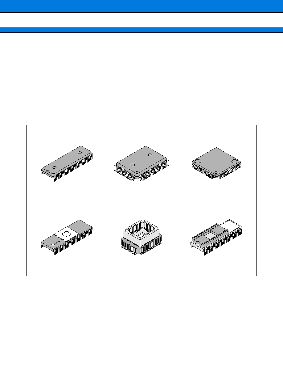
PACKAGE
64-pin Plastic SH-DIP
(DIP-64P-M01)
64-pin Ceramic SH-DIP
(DIP-64C-A06)
64-pin Plastic QFP
(FPT-64P-M06)
64-pin Ceramic MQFP
(MQP-64C-P01)
64-pin Plastic QFP
(FPT-64P-M09)
64-pin Ceramic MDIP
(MDP-64C-P02)

MB89630R Series
3
s
PRODUCT LINEUP
(Continued)
MB89636R MB89637R MB89T635R MB89T637R MB89P637 MB89W637 MB89PV630
Classification
Mass-produced products
(mask ROM products)
External ROM
products
One-time
PROM
product
EPROM
product
Piggyback/
evaluation
product (for
evaluation
and
development)
ROM size
16 K
×
8 bits
(internal
mask ROM)
24 K
×
8 bits
(internal
mask ROM)
32 K
×
8 bits
(internal
mask ROM) Fixed to external ROM
32 K
×
8 bits
(Internal PROM, to be
programmed with
general-purpose
EPROM programmer)
32 K
×
8 bits
(external
ROM)
RAM size
512
×
8 bits 768
×
8 bits 1024
×
8 bits 512
×
8 bits
1024
×
8 bits
1 K
×
8 bits
CPU functions
The number of instructionns:
136
Instruction bit length:
8 bits
Instruction length:
1 to 3 bytes
Data bit length:
1, 8, 16 bits
Minimum execution time:
0.4 to 6.4
µ
s/10 MHz, 61
µ
s@32.768 kHz
Interrupt processing time:
3.6 to 57.6
µ
s/10 MHz, 562.5
µ
s@32.768 kHz
Ports
Input ports:
5 (All also serve as peripherals.)
Output ports (N-ch open-drain):
8 (All also serve as peripherals.)
I/O ports (N-ch open-drain):
4 (All also serve as peripherals.)
Output ports (CMOS):
8 (All also serve as bus control.)
I/O ports (CMOS):
28 (27 ports also serve as bus pins and peripherals.)
Total: 53
Clock timer
21 bits
×
1 (in main clock)/15 bits
×
1 (at 32.768 kHz)
8-bit PWM
timer
8-bit reload timer operation (toggled output capable, operating clock cycle: 0.4
µ
s to 3.3 ms)
×
2
channels
7/8-bit resolution PWM operation (conversion cycle: 51.2
µ
s to 839 ms)
×
2 channels
8-bit pulse
width count
timer
8-bit timer operation (overflow output capable, operating clock cycle: 0.4 to 12.8
µ
s)
8-bit reload timer operation (toggled output capable, operating clock cycle: 0.4 to 12.8
µ
s)
8-bit pulse width measurement operation (capable of continuous measurement, and
measurement of "H" pulse width/ "L" pulse width/ from
to
/from
to
)
16-bit timer/
counter
16-bit timer operation (operating clock cycle: 0.4
µ
s)
16-bit event counter operation (rising edge/falling edge/both edge selectable)
8-bit serial I/O
8 bits
LSB first/MSB first selectable
One clock selectable from four transfer clocks
(one external shift clock, three internal shift clocks: 0.8
µ
s, 3.2
µ
s, 12.8
µ
s)
UART
Capable of switching two I/O systems by software
Transfer data length (6, 7, and 8 bits)
Transfer rate (300 to 62500 bps. at 10 MHz osciliation)
10-bit A/D
converter
10-bit resolution
×
8 channels
A/D conversion mode (conversion time: 13.2
µ
s)
Sense mode (conversion time: 7.2
µ
s)
Capable of continuous activation by an external activation or an internal timer
MB89635R
Part number
Item
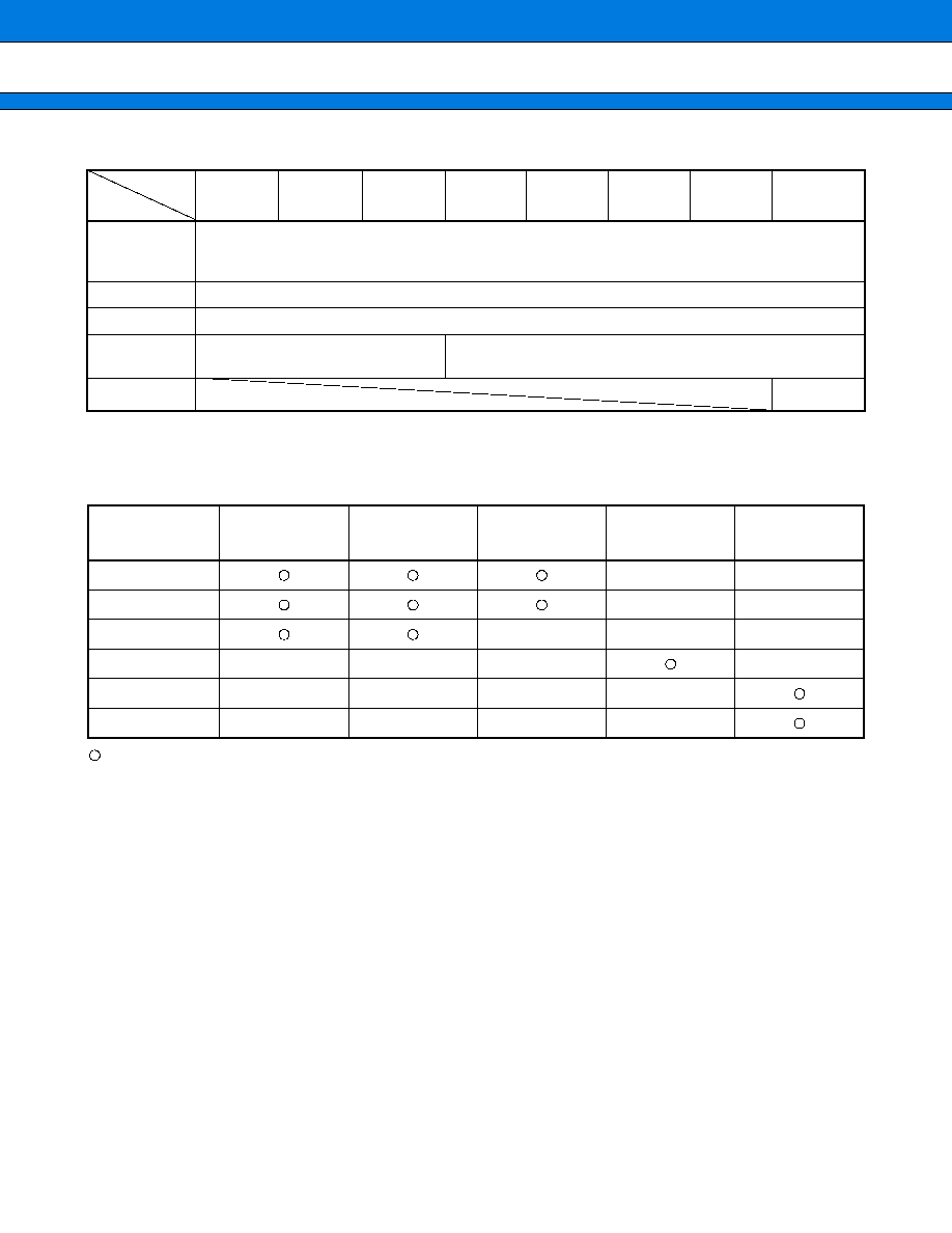
MB89630R Series
4
(Continued)
* : Varies with conditions such as the operating frequency. (See section "
s
Electrical Characteristics.")
In the case of the MB89PV630, the voltage varies with the restrictions of the EPROM for use.
s
PACKAGE AND CORRESPONDING PRODUCTS
: Available
×
: Not available
* : To convert pin pitches, an adapter socket (manufacturer: Sun Hayato Co., Ltd.) is available.
64SD-64QF2-8L: For conversion from (DIP-64P-M01, DIP-64C-A06, or MDP-64C-P02) to FPT-64P-M09
Inquiry: Sun Hayato Co., Ltd.: TEL (81)-3-3986-0403
FAX (81)-3-5396-9106
Note: For more information about each package, see section "
s
Package Dimensions."
MB89636R MB89637R MB89T635R MB89T637R MB89P637 MB89W637 MB89PV630
External
interrupt input
4 independent channels (edge selection, interrupt vector, source flag).
Rising edge/falling edge selectable
Used also for wake-up from stop/sleep mode. (Edge detection is also permitted in stop mode.)
Standby mode
Sleep mode, stop mode, watch mode, and subclock mode
Process
CMOS
Operating
voltage*
2.2 V to 6.0 V
2.7 V to 6.0 V
EPROM for use
MBM27C256A-20CZ
MBM27C256A-20TV
Package
MB89635R
MB89T635R
MB89636R
MB89637R
MB89T637R
MB89P637
MB89W637
MB89PV630
DIP-64P-M01
×
×
FPT-64P-M06
×
×
FPT-64P-M09
×
*
×
*
×
*
DIP-64C-A06
×
×
×
×
MQP-64C-P01
×
×
×
×
MDP-64C-P02
×
×
×
×
MB89635R
Part number
Item

MB89630R Series
5
s
DIFFERENCES AMONG PRODUCTS
1. Memory Size
Before evaluating using the piggyback product, verify its differences from the product that will actually be used.
Take particular care on the following points:
On the MB89P637/W637, the program area starts from address 8007
H
but on the MB89PV630 and MB89637R
starts from 8000
H
.
· On the MB89P637/W637, addresses 8000
H
to 8006
H
comprise the option setting area, option settings can be
read by reading these addresses. On the MB89PV630/MB89637R, addresses 8000
H
to 8006
H
could also be
used as a program ROM. However, do not use these addresses in order to maintain compatibility of the
MB89P637/W637.
· The stack area, etc., is set at the upper limit of the RAM.
· The external area is used.
2. Current Consumption
· In the case of the MB89PV630, add the current consumed by the EPROM which connected to the top socket.
· When operated at low speed, the product with an OTPROM (one-time PROM) or an EPROM will consume
more current than the product with a mask ROM. However, the current consumption in sleep/stop modes is
the same. (For more information, see sections "
s
Electrical Characteristics" and "
s
Example Characteristics.")
3. Mask Options
Functions that can be selected as options and how to designate these options vary by the product.
Before using options check section "
s
Mask Options."
Take particular care on the following points:
· A pull-up resistor cannot be set for P50 to P53 on the MB89P637 and MB89W637.
· Options are fixed on the MB89PV630, MB89T635R, and MB89T637R.
4. Differences between the MB89630 and MB89630R Series
· Memory access area
There are no difference between the access area of MB89635/MB89635R, and that of MB89637/MB89637R.
The access area of MB89636 is different from that of the MB89636R when using in external bus mode.
Address
Memory area
MB89636
MB89636R
0000
H
to 007F
H
I/O area
I/O area
0080
H
to 037F
H
RAM area
RAM area
0380
H
to 047F
H
External area
Access prohibited
0480
H
to 7FFF
H
External area
8000
H
to 9FFF
H
Access prohibited
A000
H
to FFFF
H
ROM area
ROM area