
DS07-12512-8E
FUJITSU SEMICONDUCTOR
DATA SHEET
8-bit Proprietary Microcontroller
CMOS
F
2
MC-8L MB89190/190A Series
MB89191/193/195/P195/PV190
MB89191A/191AH/193A/193AH/195A/P195A/PV190A
s
OUTLINE
The MB89190/190A series microcontrollers contain various resources such as timers, serial interfaces, A/D
converters, external interrupts, and remote-control functions, as well as an F
2
MC*-8L CPU core for low-voltage
and high-speed operations. These single-chip microcontrollers are suitable for small devices such as remote
controllers with compact packages.
*: F
2
MC stands for FUJITSU Flexible Microcontroller.
s
FEATURES
Ę Minimum execution time: 0.95
Ą
s at 4.2 MHz (V
CC
= 2.7 V)
Ę F
2
MC-8L family CPU core
Ę Two timers
8/16-bit timer/counter
20-bit timebase counter
Ę Serial interface
8-bit synchronous serial (Selectable transfer direction allows communication with various equipment.)
(Continued)
s
PACKAGE
28-pin Plastic SOP
(FPT-28P-M17)
28-pin Plastic DIP
(DIP-28P-M05)
28-pin Plastic SH-DIP
(DIP-28P-M03)
48-pin Ceramic MQFP
(MQP-48C-P01)
MB89190/190A Series
2
(Continued)
Ę External interrupts
Edge detection (Selectable edge): 3 channels
Low-level interrupt (Wake-up function): 8 channels
Ę A/D converter (MB89190A series only)
8-bit successive approximation type: 8 channels
Ę Built-in remote-control transmitting frequency generator
Ę Low-power consumption modes
Stop mode (Almost no current consumption occurs because oscillation stops.)
Sleep mode (The current consumption is reduced about 1/3 of that during normal operation because the CPU
stops.)
Ę Packages
SOP-28, SH-DIP-28, and DIP-28
s
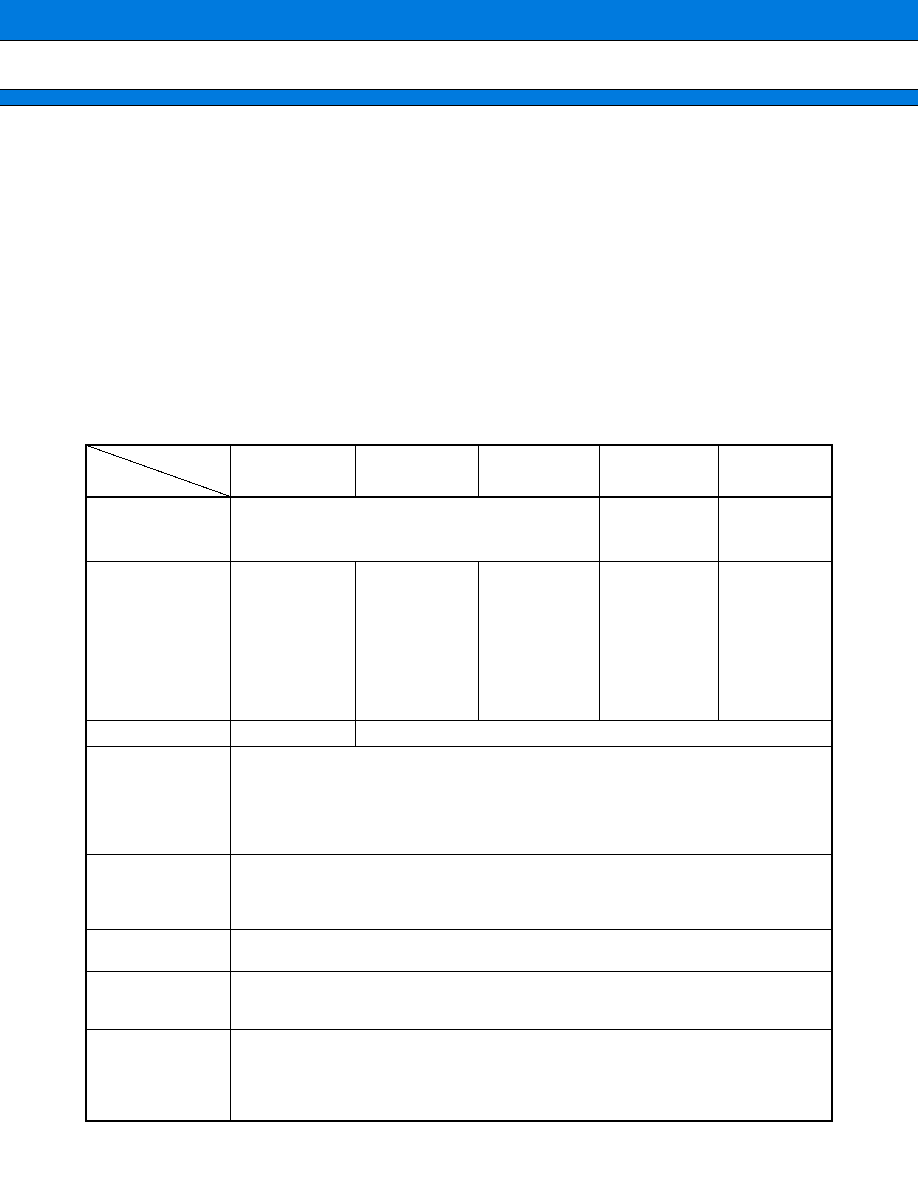
PRODUCT LINEUP
Part number
Item
MB89191
MB89191A
MB89191AH
MB89193
MB89193A
MB89193AH
MB89195
MB89195A
MB89P195
MB89P195A
MB89PV190
MB89PV190A
Classification
Mask ROM products
One-time
product
For
development
and evaluation
ROM size
4 K
ū
8 bits
(internal mask
ROM)
8 K
ū
8 bits
(internal mask
ROM)
16 K
ū
8 bits
(internal mask
ROM)
16 K
ū
8 bits
(internal PROM,
to be
programmed
with general-
purpose
EPROM
programmer)
32 K
ū
8 bits
(external ROM)
RAM size
128
ū
8 bits
256
ū
8 bits
CPU functions
The number of basic instructions:
136
Instruction bit length:
8 bits
Instruction length:
1 to 3 bytes
Data bit length:
1, 8, and 16 bits
Minimum execution time:
0.95
Ą
s at 4.2 MHz
Interrupt processing time:
8.57
Ą
s at 4.2 MHz
Ports
Output port (N channel open drain): 4 (also serves as peripherals for MB89190A
series)or 6 (for MB89190 series)
I/O port (CMOS):
16 (also serves as peripherals)
Total:
20 or 22
Timer counter
2 channels of 8-bit timer counter or one 16-bit event counter (operation clock: 1.9
Ą
s, 30.4
Ą
s, and 487.6
Ą
s at 4.2 MHz, and external clock)
Serial I/O
8 bits
LSB/MSB first selectable
Transfer clock (external, 1.9
Ą
s, 7.6
Ą
s, 30.4
Ą
s at 4.2 MHz)
A/D converter
(MB89190A series
only)
8 bits x 8 channels
A/D conversion mode (conversion time: 41.9
Ą
s at 4.2 MHz)
Sense mode (conversion time: 11.9
Ą
s at 4.2 MHz)
Capable of continuous activation by an internal timer.
Reference voltage input
(Continued)
MB89190/190A Series
3
*: Varies with conditions such as operating frequencies (see "
s
Electrical Characteristics.") It differs from the
operating voltage of an A/D converter.
s
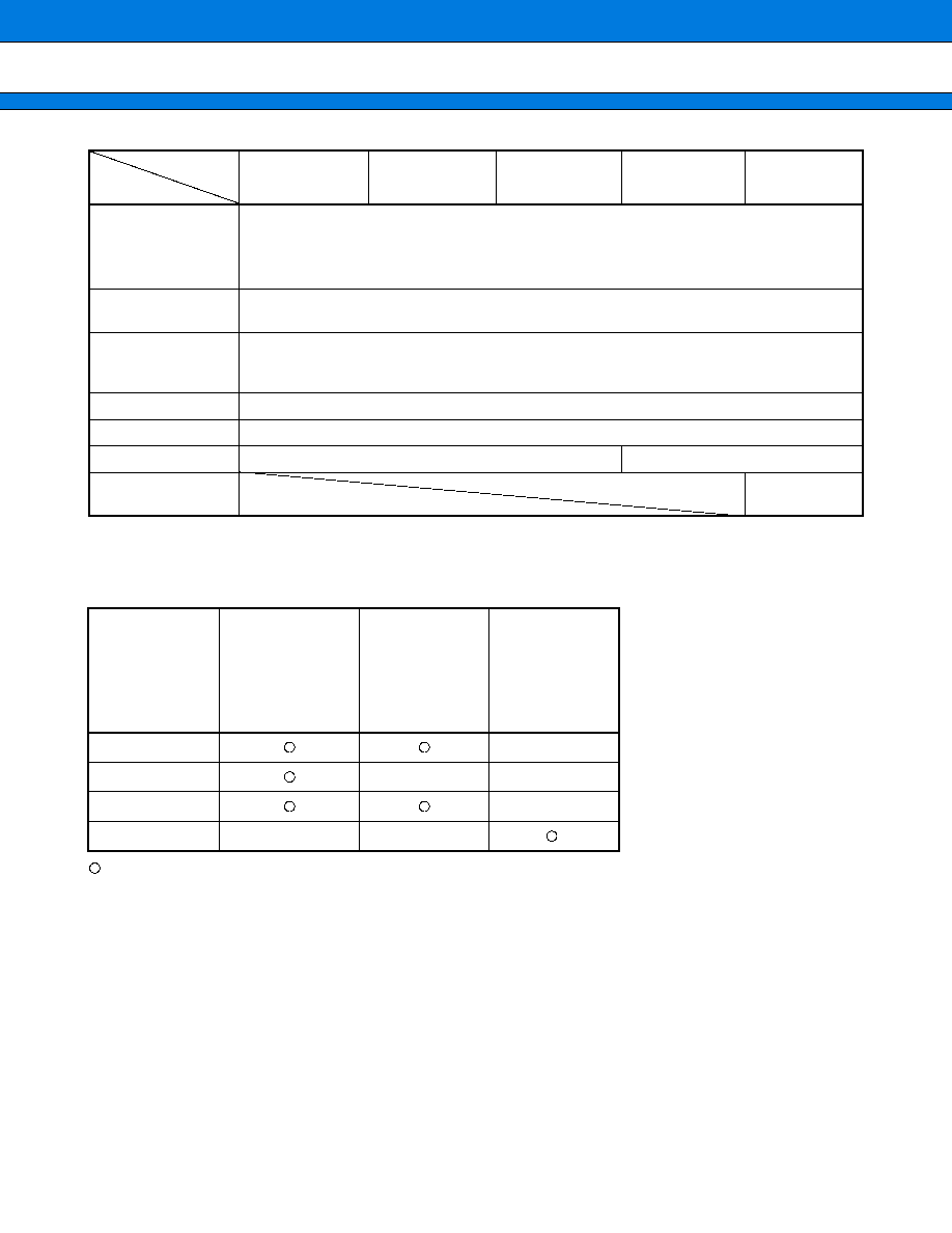
PACKAGE AND CORRESPONDING PRODUCTS
: Available
ū
: Not available
* : A socket (manufacturer: Sun Hayato Co., Ltd.) for pin pitch conversion is available.
48QF-28SOP-8L: (MQP-48C-P01)
for conversion to FPT-28P-M17
Inquiry: Sun Hayato Co., Ltd.: TEL (81)-3-3986-0403
FAX (81)-3-5396-9106
Note: For more information on each package, see "
s
Package Dimensions."
External interrupt 1
3 independent channels (selectable edge, interrupt vector, and interrupt source flag)
Rising/falling/both edge selectable
Used for wake-up from stop/sleep mode. (Edge detection is also permitted in the stop
mode.)
External interrupt 2
(Wake-up function)
8 channels (low-level interrupt only)
Remote-control
transmitting
frequency generator
The pulse width and cycle are software-programmable.
Standby mode
Sleep mode and stop mode
Process
CMOS
Operating voltage*
2.2 V to 6.0 V
2.7 V to 6.0 V
EPROM for use
MBM27C256A-
20TVM
Package
MB89191
MB89191A
MB89191AH
MB89193
MB89193A
MB89193AH
MB89195
MB89195A
MB89P195
MB89P195A
MB89PV190
MB89PV190A
DIP-28P-M05
ū
DIP-28P-M03
ū
ū
FPT-28P-M17
ū
MQP-48C-P01
ū
ū
*
Part number
Item
MB89191
MB89191A
MB89191AH
MB89193
MB89193A
MB89193AH
MB89195
MB89195A
MB89P195
MB89P195A
MB89PV190
MB89PV190A
(Continued)

MB89190/190A Series
4
s
DIFFERENCES AMONG PRODUCTS
1. Memory Size
Before evaluating using the piggyback model, verify its difference from the model that will actually be used.
Take particular care on the following points:
Ę On the MB89191/191A, addresses 0140
H
to 0180
H
cannot be used for register banks.
Ę The stack area, etc., is set in the upper limit of the RAM.
2. Current Consumption
Ę In the case of MB89PV190/PV190A, added is the current consumed by the EPROM which is connected to
the top socket.
Ę When operated at low speed, the products with an OTPROM (EPROM) will consume more current than the
products with a mask ROM.
However, the same is current consumption in the sleep/stop mode. (For more information, see "
s
Electrical
Characteristics.")
3. Mask Options
Functions that can be selected as options and how to designate these options vary with product.
Before using options, check "
s
Mask Options."
Take particular care on the following points:
Ę Pull-up resistor optional cannot be set for P00 to P03, and P40 to P45 on the MB89191A/193A/195A/P195A.
Ę The power-on reset option is fixed as "enabled" for MB89P195/P195A.
Ę Options are fixed on the MB89PV190/PV190A.
4. MB89191AH/MB89193AH
MB89191AH/193AH are "L" level heavy output current drive type of P30 to P32 and P40 to P43 of MB89191A/
193A.Characteristics other than "L" level output of P30 to P32 and P40 to P43 are the same as MB89191A/193A.

MB89190/190A Series
5
s
PIN ASSIGNMENT
1
2
3
4
5
6
7
8
9
10
11
12
13
14
V
CC
P03/INT23/AN7
P02/INT22/AN6
P01/INT21/AN5
P00/INT20/AN4
P45/AVR
P44/AV
SS
P43/AN3
P42/AN2
P41/AN1
P40/AN0
P30/SCK
P31/SO
P32/SI
P04/INT24
P05/INT25
P06/INT26
P07/INT27
TEST
RST
X0
X1
V
SS
P37/BZ/RCO
P36/INT12
P35/INT11
P34/TO/INT10
P33/EC
28
27
26
25
24
23
22
21
20
19
18
17
16
15
(TOP VIEW)
(FPTŁ28PŁM17)
(DIPŁ28PŁM03)
(DIPŁ28PŁM05)