Document Outline
- DESCRIPTION
- FEATURES
- PACKAGE
- PIN ASSIGNMENT
- PIN DESCRIPTION
- BLOCK DIAGRAM
- ABSOLUTE MAXIMUM RAGINGS (See WARNING)
- RECOMMENDED OPERATING CONDITIONS
- ELECTRIC CHARACTERISTICS
- EVALUATION BOARD (Reference Example)
- MEASUREMENT DATA (Reference Values)
- 800-MHz PDC APPLICATION MEASUREMENT DATA (Reference Values)
- TEST CIRCUITS (Reference Examples)
- ORDERING INFORMATION
- PACKAGE DIMENSION

1
DS04-23509-1E
FUJITSU SEMICONDUCTOR
DATA SHEET
ASSP
for Telephone
BIPOLAR
Quadrature Modulator IC
(With 1.0 GHz Up-converter)
MB54609
s
DESCRIPTION
The MB54609 is an intermediate-frequency (IF) quadrature modulator IC incorporating a 1.0-GHz up-converter
optimized for use in digital mobile telecommunication systems such as GSM and PDC (Personal Digital Cellular).
The MB54609 incorporates a quadrature modulator for IF modulation, a transmission up-convert mixer, and a
F/F type phase shifter as well, capable of handing IFs in a broad band.
In addition, the MB54609 operates at a low power supply voltage of 3.0 V and a low power supply current of 18
mA (both as typical values), contributing to saving the power consumption of the device.
s
FEATURES
Ě Incorporating a high-performance transmission mixer covering the entire frequency band of up to 800 MHz used
for PDC services (Maximum output frequency of 1.1 GHz)
Maximum output frequency: 1.1 GHz, Output level: ş9 dBm (typical)
Ě Externally connecting the quadrature modulator with the transmission mixer, allowing a bandpass filter (BPF)
to be inserted in between
The quadrature modulator output can drive a 50
load.
Ě Flip-flop phase shifter capable of handling intermediate frequencies in the broad band (100 to 800 MHz)
Ě Operation at low voltage: 2.7 to 3.0 to 3.3 V
Ě Low current consumption
During operating: 18.0 mA (typical)
In power save mode: 0.6 mA (typical)
Ě Operating temperature range: Ta = ş20 to +85░C
s
PACKAGE
20-pin Plastic SSOP
(FPT-20P-M03)
2
MB54609
s
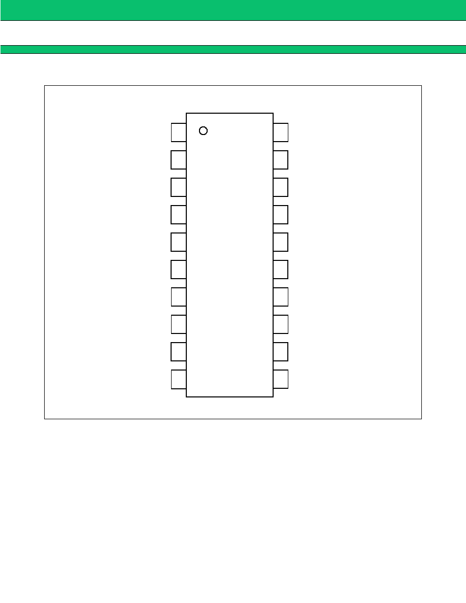
PIN ASSIGNMENT
RFout
GND
LO2
GND
XIF
IF
LO1
XLO1
GND
V
CC
V
CC
GND
I
XI
QMOD
XQMOD
XQ
Q
GND
PS
1
2
3
4
5
6
7
8
9
10
11
12
13
14
15
16
17
18
19
20
(FPT-20P-M03)
(TOP VIEW)

3
MB54609
s
PIN DESCRIPTION
Pin no.
Pin name
Function
1
RFout
Up-converter output pin
2
GND
GND pin
3
LO2
LO input pin for mixer
4
GND
GND pin
5
XIF
IF input complementary pin for mixer
6
IF
IF input pin for mixer
7
LO1
LO input pin for quadrature modulator
8
XLO1
LO input complementary pin for quadrature modulator
9
GND
GND pin
10
V
CC
Power supply pin
Power supply voltage must be applied to both pins.
11
V
CC
Power supply pin
12
GND
GND pin
13
I
Baseband input (I) pin
14
XI
Baseband input (I) complementary pin
15
QMOD
Quadrature modulator IF output pin
16
XQMOD
Quadrature modulator IF output complementary pin
17
XQ
Baseband input (Q) complementary pin
18
Q
Baseband input (Q) pin
19
GND
GND pin
20
PS
Power save mode control pin
4
MB54609
s
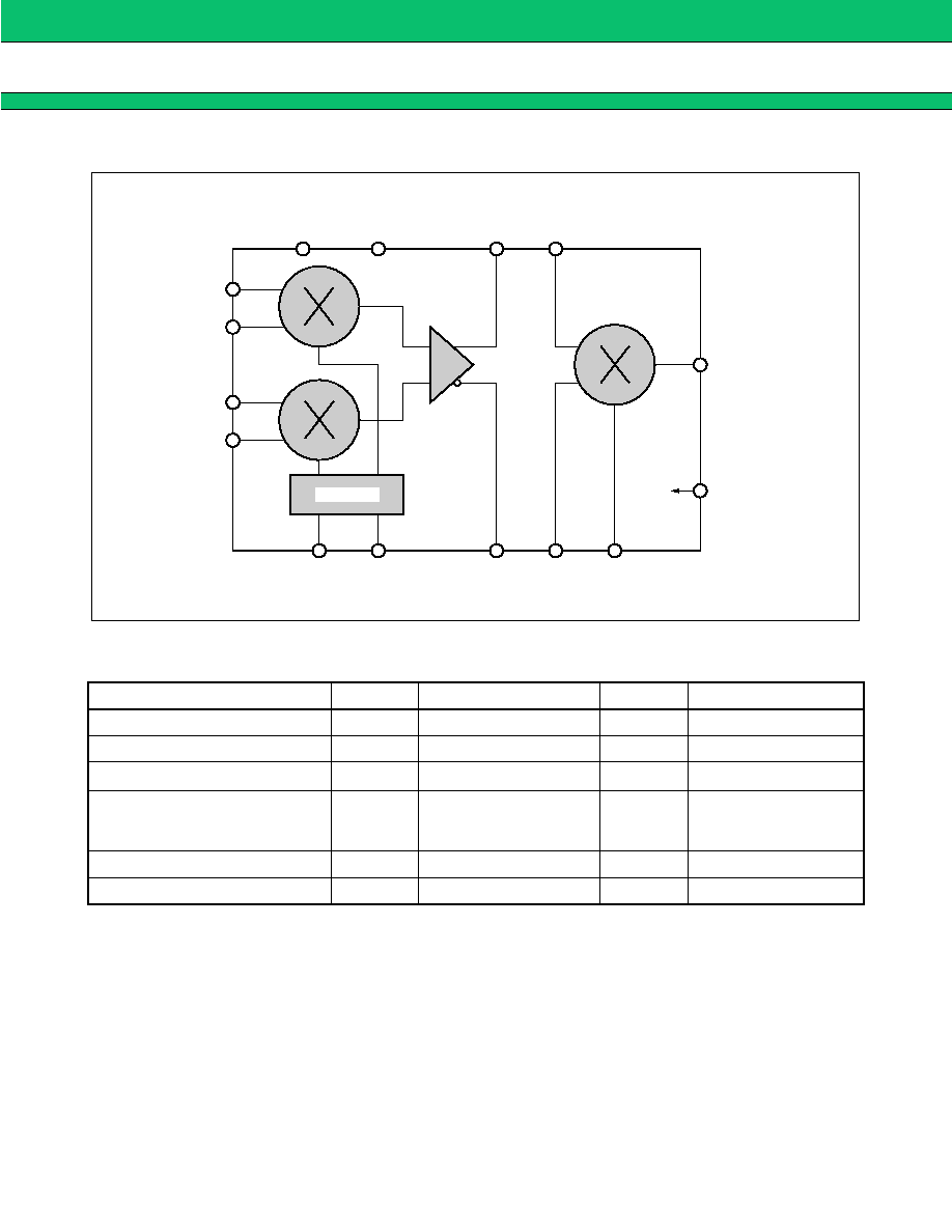
BLOCK DIAGRAM
s
ABSOLUTE MAXIMUM RAGINGS (See WARNING)
WARNING: Exceeding any of the above Absolute Maximum Ratings may cause permanent damage to the LSI.
For normal operation, the device should be used under the recommended operating conditions.
Exceeding any of the recommended conditions may adversely affect LSI reliability.
Note: Although the MB54609 contains an antistatic element to prevent electrostatic breakdown and the circuitry
has been improved in electrostatic protection, observe the following precautions when handling the device:
Ě When storing or carrying the device, put it in a conductive case.
Ě Before handling the device, check that the jigs and tools to be used have been uncharged (grounded) as
well as yourself. Use a conductive sheet on the working bench.
Ě Before fitting the device into or removing it from the socket, turn the power supply off.
Ě When handling (such as transporting) the MB54609 mounted board, protect the leads with a conductive
sheet.
Parameter
Symbol
Rating
Unit
Remarks
Power supply voltage
V
CC
ş0.5 to 5.0
V
Output voltage
V
O
ş0.5 to V
CC
+ 0.5
V
Input voltage
V
I
ş0.5 to V
CC
+ 0.5
V
Open collector applied voltage
V
OC
V
CC
▒ 0.3
(ş0.5 to 5.0)
V
RFout pin
Do not leave this pin
open.
Output current
I
O
▒10
mA
Storage temperature
Tstg
ş55 to +125
░
C
RFout
GND
LO2
XIF
IF
XLO1
LO1
V
CC
I
XI
QMOD
XQMOD
XQ
Q
PS
90░ shifter

5
MB54609
s
RECOMMENDED OPERATING CONDITIONS
s
ELECTRIC CHARACTERISTICS
(V
CC
= 3.0 V, Ta = +25
░
C)
Parameter
Symbol
Value
Unit
Remarks
Min.
Typ.
Max.
Power supply voltage
V
CC
2.7
3.0
3.3
V
Input voltage
V
I
GND
--
V
CC
V
Open collector applied voltage
V
OC
V
CC
ş 0.2
--
V
CC
+ 0.2
V
RFout pin. Do not leave
this pin open.
Operating temperature
T
a
ş20
--
+85
░
C
Parameter
Symbol
Value
Unit
Remarks
Min.
Typ.
Max.
Power supply current
I
CC
--
18.0
23.5
mA
DC current (Input with no AC
signal)
Power supply current in power save
mode
I
CC
PS
--
0.6
0.9
mA
DC current (Input with no AC
signal)
Shifter input
LO1
Operating band
f
LO1
100
400
800
MHz
Input level
P
LO1
ş15
--
ş5
dBm
Baseband
input
Operating band
f
BB
DC
--
10
MHz
Input amplitude
V
BB
--
--
1.2
Vpp
Offset voltage
V
OS
1.5
1.6
1.7
V
External offset voltage value
Offset current
I
OS
--
3.0
--
Á
A
Input Imp. converted value =
533 k
Mixer input
LO2
Operating band
f
LO2
--
750
1100
MHz
Input level
P
LO2
--
--
0
dBm
Mixer output
RFout
Operating band
f
RF
--
950
1100
MHz
f
RF
= f
LO2
▒ f
LO1
/2
Output level
P
RF
--
ş9
--
dBm
--
f
LO1
= 400 MHz
(ş15 dBm)
f
LO2
= 750 MHz
(ş5 dBm)
f
RF
= 950 MHz
output
QMOD/Mix direct
connection
V
BB
= 1 Vpp
Modulation
precision
Amplitude deviation
A
ERR
--
1.3
--
%
RMS
value
Phase deviation
P
ERR
--
0.82
--
deg.
RMS
value
Vector error
V
ERR
--
1.9
--
%
RMS
value
Carrier suppression
CS
--
ş40
ş30
dBc
With external offset
unadjusted