H04-004-07
Fuji Electric Co.,Ltd.
Matsumoto Factory
SPECIFICATION
Device Name :
Type Name :
Spec. No. :
IGBT Module
6MBI75UB-120
MS5F 5497
1
13
MS5F 5497
Jun. 18 '03 Y.Kobayashi
T.Miyasaka
K.Yamada
T.Fujihira
Jun. 18 '03

H04-004-06
R e v i s e d R e c o r d s
Date
Classi-
fication
Ind.
Content
Applied
date
Drawn
Checked
Approved
enactment
Issued
date
MS5F 5497
2
13
T.Miyasaka
K.Yamada
T.Fujihira
Jun.- 18 -'03
H04-004-03
13
MS5F 5497
3
6MBI75UB-120
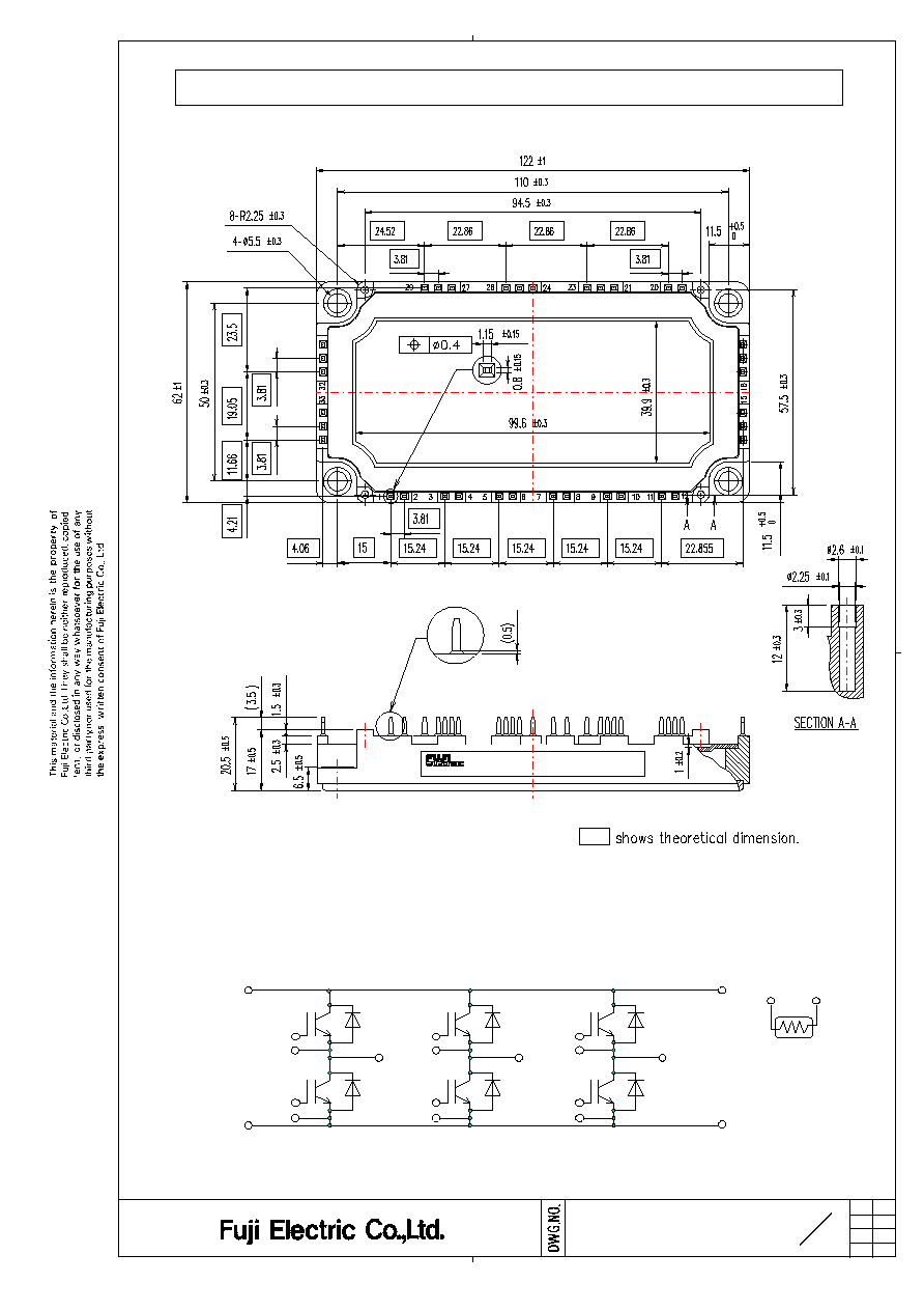
2. Equivalent circuit
1. Outline Drawing ( Unit : mm )
U
V
W
1
2
3
4
5
6
7
8
9
10
11
12
13,14,15
16,17,18
21,22,23
24,25,26
19
20
27,28,29
30,31,32
33,34,35
( ) shows reference dimension.
H04-004-03
13
MS5F 5497
4
3.Absolute Maximum Ratings ( at Tc= 25 unless otherwise specified
Tc=25
Tc=80
Tc=25
Tc=80
(*1) All terminals should be connected together when isolation test will be done.
(*2) Two termistor terminals should be connected together, each other terminals should be connected together
and shorted to base plate when isolation test will be done.
(*3) Recommendable Value : 2.5~3.5 Nm (M5)
4. Electrical characteristics ( at Tj= 25 unless otherwise specified)
(*)
Biggest internal terminal resistance among arm.
3.4
-
m
Lead resistance, terminal-chip *
R lead
-
Inverter
IGES
Zero gate voltage
Collector current
ICES
ton
tr
tr (i)
Collector-Emitter
saturation voltage
VGE=15V
Ic = 75A
VGE = 0V
toff
tf
Rg = 9.1
VGE(th)
520
Turn-on time
Turn-off time
Gate-Emitter
leakage current
Gate-Emitter
threshold voltage
VGE=0V
VCE(sat)
(
terminal)
-
-
2.00
�s
IF = 75A
-
5000
-
-
0.35
T =100
465
-
1.60
1.90
Tj=125
-
Reverse recovery time
-
VF
(chip)
Tj= 25
-
Tj=125
IF = 75A
�s
Forward on voltage
VF
(terminal)
Tj= 25
-
1.90
2.20
V
1.70
1.00
1.20
0.60
-
-
0.36
-
0.21
Vcc = 600V
Ic = 75A
VGE=�15V
1200
Ic
Icp
100
75
200
150
V
�20
V
Items
Symbols
Conditions
VCES
Collector-Emitter voltage
VGES
AC : 1min.
Continuous
1ms
2500
VAC
Nm
-Ic pulse
Pc
Tj
A
W
1 device
150
Gate-Emitter voltage
Collector current
Junction temperature
Collector Power Dissipation
-Ic
75
150
390
1ms
Units
max.
typ.
Screw
Torque
-
min.
Characteristics
Tstg
Mounting *3
3.5
Conditions
between terminal and copper base *1
between thermistor and others *2
Storage temperature
Isolation
voltage
Viso
-40 +125
Ic = 75mA
200
VCE = 20V
Items
Symbols
VGE=�20V
VCE = 0V
-
-
-
nA
1.0
mA
V
-
8.5
V
4.5
6.5
Units
-
1.75
2.10
Maximum
Ratings
-
2.05
2.40
-
2.30
2.00
-
-
0.03
-
0.37
-
0.07
0.30
Input capacitance
Cies
VCE=10V,VGE=0V,f=1MHz
-
8
-
nF
K
Thermistor
Resistance
R
T = 25
B
3305
3375
3450
495
VCE = 1200V
-
B value
T = 25/50
VCE(sat)
(chip)
Tj= 25
Tj=125
Tj= 25
Tj=125
-
H04-004-03
13
MS5F 5497
5
5. Thermal resistance characteristics
This is the value which is defined mounting on the additional cooling fin with thermal compound.
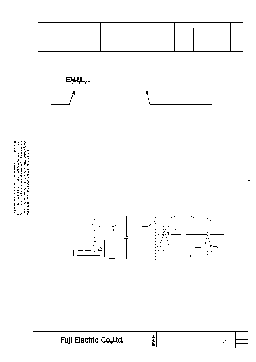
6. Indication on module
7.Applicable category
This specification is applied to IGBT Module named 6MBI75UB-120 .
8.Storage and transportation notes
The module should be stored at a standard temperature of 5 to 35 and humidity of 45 to 75% .
Store modules in a place with few temperature changes in order to avoid condensation on the module surface.
Avoid exposure to corrosive gases and dust.
Avoid excessive external force on the module.
Store modules with unprocessed terminals.
Do not drop or otherwise shock the modules when transporting.
9. Definitions of switching time
10. Packing and Labeling
Display on the packing box
- Logo of production
- Type name
- Lot No
- Products quantity in a packing box
Lot.No.
Items
Symbols
Conditions
Characteristics
Units
min.
typ.
max.
FWD
-
Thermal resistance(1device)
Contact Thermal resistance(1device)
Rth(j-c)
Rth(c-f)
with Thermal Compound ()
-
-
0.05
Place of manufacturing (code)
/W
75A 1200V
6MBI75UB-120
-
0.32
-
-
0.49
IGBT
L
Vcc
Ic
V
CE
R
G
V
GE
V
GE
V
CE
Ic
0V
0A
0V
10%
90%
10%
10%
90%
90%
0V
Ic
V
CE
on
on
on
on
t
t
t
t
r
r
r
r
t
t
t
t
r(i)
r(i)
r(i)
r(i)
t
t
t
t
off
off
off
off
t
t
t
t
f
f
f
f
t
t
t
t
rr
rr
rr
rr
I
I
I
I
rr
rr
rr
rr
t
t
t
t
H04-004-03
13
MS5F 5497
11. Reliability test results
6
Reliability Test Items
Test
cate-
gories
Test items
Test methods and conditions
Reference
norms
EIAJ ED-4701
(Aug.-2001 edition)
Number
of
sample
Accept-
ance
number
1 Terminal Strength Pull force
: 20N
Test Method 401
5
( 0 : 1 )
(Pull test)
Test time
: 10�1 sec.
Method
2 Mounting Strength Screw torque
: 2.5 ~ 3.5 Nm (M5)
Test Method 402
5
( 0 : 1 )
Test time
: 10�1 sec.
method
3 Vibration
Range of frequency : 10 ~ 500Hz
Test Method 403
5
( 0 : 1 )
Sweeping time
: 15 min.
Reference 1
Acceleration
: 100m/s
2
Condition code B
Sweeping direction : Each X,Y,Z axis
Test time
: 6 hr. (2hr./direction)
4 Shock
Maximum acceleration : 5000m/s
2
Test Method 404
5
( 0 : 1 )
Pulse width
: 1.0msec.
Condition code B
Direction
: Each X,Y,Z axis
Test time
: 3 times/direction
5 Solderabitlity
Solder temp.
: 235�5
Test Method 303
5
( 0 : 1 )
Immersion time
: 5�0.5sec.
Condition code A
Test time
: 1 time
Each terminal should be Immersed in solder
within 1~1.5mm from the body.
6 Resistance to
Solder temp.
: 260�5
Test Method 302
5
( 0 : 1 )
Soldering Heat
Immersion time
: 10�1sec.
Condition code A
Test time
: 1 time
Each terminal should be Immersed in solder
within 1~1.5mm from the body.
1 High Temperature Storage temp.
: 125�5
Test Method 201
5
( 0 : 1 )
Storage
Test duration
: 1000hr.
2 Low Temperature Storage temp.
: -40�5
Test Method 202
5
( 0 : 1 )
Storage
Test duration
: 1000hr.
3 Temperature
Storage temp.
: 85�2
Test Method 103
5
( 0 : 1 )
Humidity
Relative humidity
: 85�5%
Test code C
Storage
Test duration
: 1000hr.
4 Unsaturated
Test temp.
: 120�2
Test Method 103
5
( 0 : 1 )
Pressure Cooker Atmospheric pressure : 1.7 � 10
5
Pa
Test code E
Test humidity
: 85�5%
Test duration
: 96hr.
5 Temperature
Test Method 105
5
( 0 : 1 )
Cycle
Test temp.
: Low temp. -40�5
High temp. 125 �5
RT 5 ~ 35
Dwell time
: High ~ RT ~ Low ~ RT
1hr. 0.5hr. 1hr. 0.5hr.
Number of cycles
: 100 cycles
6 Thermal Shock
+0
Test Method 307
5
( 0 : 1 )
Test temp.
: High temp. 100
-5
method
+5
Condition code A
Low temp. 0
-0
Used liquid : Water with ice and boiling water
Dipping time
: 5 min. par each temp.
Transfer time
: 10 sec.
Number of cycles
: 10 cycles
Mechanical Tests
Environment Tests
H04-004-03
13
MS5F 5497
7
Reliability Test Items
Test
cate-
gories
Test items
Test methods and conditions
Reference
norms
EIAJ ED-4701
(Aug.-2001 edition)
Number
of
sample
Accept-
ance
number
1 High temperature
Test Method 101
5
( 0 : 1 )
Reverse Bias
Test temp.
: Ta = 125�5
(Tj
150 )
Bias Voltage
: VC = 0.8�VCES
Bias Method
: Applied DC voltage to C-E
VGE = 0V
Test duration
: 1000hr.
2 High temperature
Test Method 101
5
( 0 : 1 )
Bias (for gate)
Test temp.
: Ta = 125�5
(Tj
150 )
Bias Voltage
: VC = VGE = +20V or -20V
Bias Method
: Applied DC voltage to G-E
VCE = 0V
Test duration
: 1000hr.
3 Temperature
Test Method 102
5
( 0 : 1 )
Humidity Bias
Test temp.
: 85�2
o
C
Condition code C
Relative humidity
: 85�5%
Bias Voltage
: VC = 0.8�VCES
Bias Method
: Applied DC voltage to C-E
VGE = 0V
Test duration
: 1000hr.
4 Intermitted
ON time
: 2 sec.
Test Method 106
5
( 0 : 1 )
Operating Life
OFF time
: 18 sec.
(Power cycle)
Test temp.
: Tj=100�5 deg
( for IGBT )
Tj
150 , Ta=25�5
Number of cycles
: 15000 cycles
Endurance Tests
Failure Criteria
Item
Characteristic
Symbol
Failure criteria
Unit
Note
Lower limit Upper limit
Electrical
Leakage current
ICES
-
USL�2
mA
characteristic
�IGES
-
USL�2
�A
Gate threshold voltage VGE(th)
LSL�0.8
USL�1.2
mA
Saturation voltage
VCE(sat)
-
USL�1.2
V
Forward voltage
VF
-
USL�1.2
V
Thermal
IGBT
VGE
-
USL�1.2
mV
resistance
or
VCE
FWD
VF
-
USL�1.2
mV
Isolation voltage
Viso
Broken insulation
-
Visual
Visual inspection
inspection
Peeling
-
The visual sample
-
Plating
and the others
LSL : Lower specified limit.
USL : Upper specified limit.
Note : Each parameter measurement read-outs shall be made after stabilizing the components
at room ambient for 2 hours minimum, 24 hours maximum after removal from the tests.
And in case of the wetting tests, for example, moisture resistance tests, each component
shall be made wipe or dry completely before the measurement.
Each parameter measurement read-outs shall be made after stabilizing the components
at room ambient for 2 hours minimum, 24 hours maximum after removal from the tests.
And in case of the wetting tests, for example, moisture resistance tests, each component
shall be made wipe or dry completely before the measurement.
H04-004-03
13
MS5F 5497
8
Reliability Test Results
Test
cate-
gorie
s
Test items
Reference
norms
EIAJ ED-4701
(Aug.-2001 edition)
Number
of test
sample
Number
of
failure
sample
1 Terminal Strength
Test Method 401
5
0
(Pull test)
Method
2 Mounting Strength
Test Method 402
5
0
method
3 Vibration
Test Method 403
5
0
Condition code B
4 Shock
Test Method 404
5
0
Condition code B
5 Solderabitlity
Test Method 303
5
0
Condition code A
6 Resistance to Soldering Heat
Test Method 302
5
0
Condition code A
1 High Temperature Storage
Test Method 201
5
0
2 Low Temperature Storage
Test Method 202
5
0
3 Temperature Humidity
Test Method 103
5
0
Storage
Test code C
4 Unsaturated
Test Method 103
5
0
Pressure Cooker
Test code E
5 Temperature Cycle
Test Method 105
5
0
6 Thermal Shock
Test Method 307
5
0
method
Condition code A
1 High temperature Reverse Bias
Test Method 101
5
0
2 High temperature Bias
Test Method 101
5
0
( for gate )
3 Temperature Humidity Bias
Test Method 102
5
0
Condition code C
4 Intermitted Operating Life
Test Method 106
5
0
(Power cycling)
( for IGBT )
Endurance Tests
Mechanical Tests
Environment Tests
H04-004-03
13
MS5F 5497
9
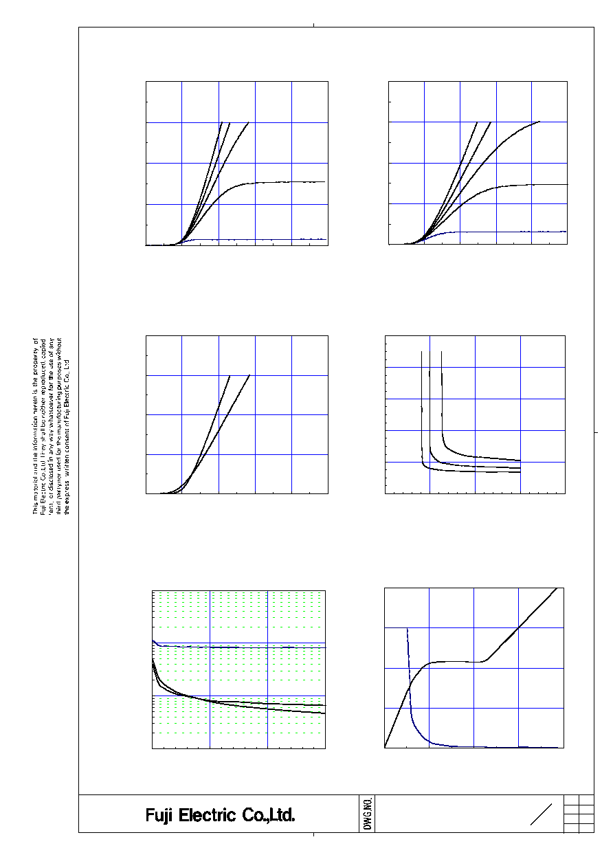
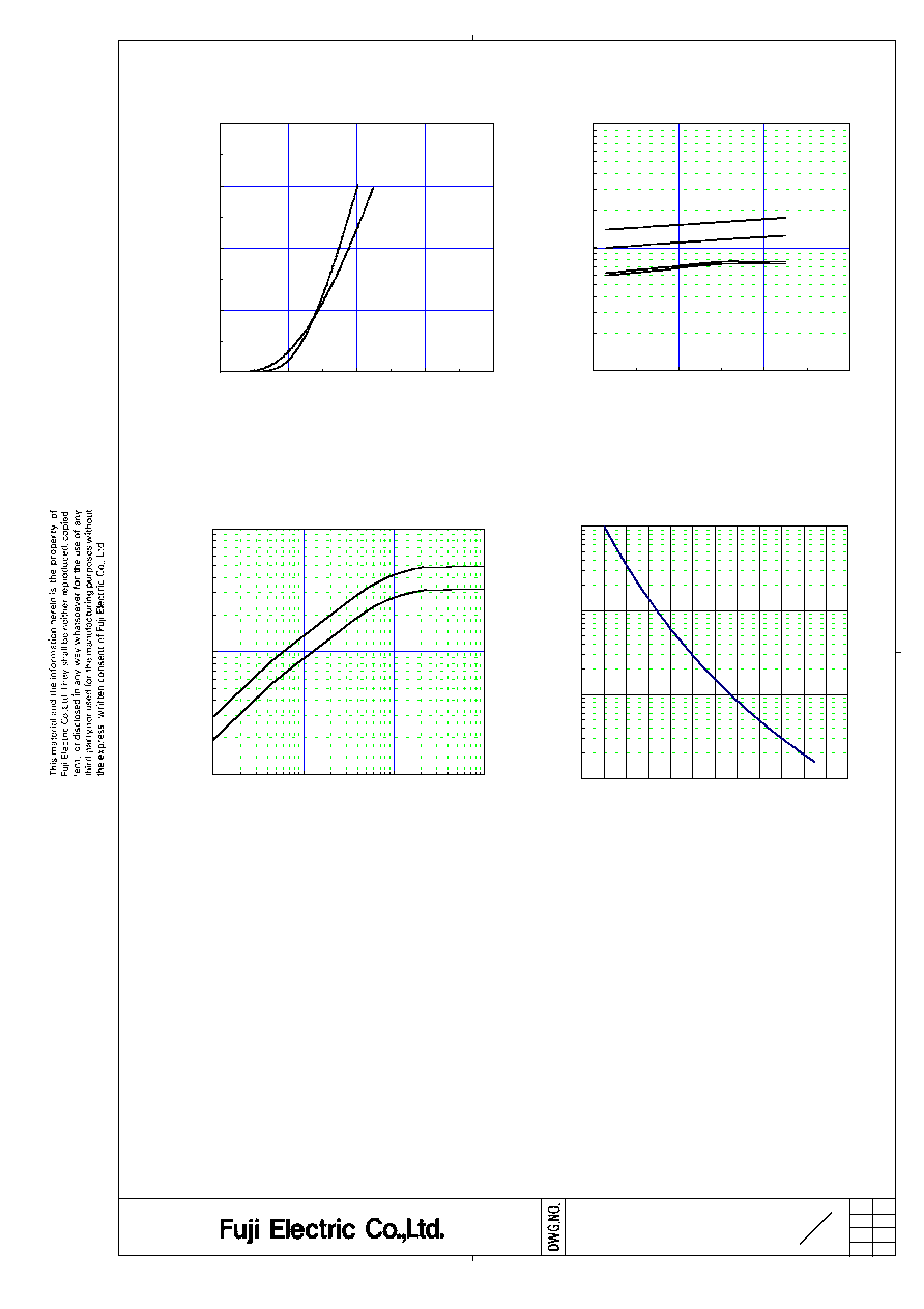
Vcc=600V Ic=75ATj= 25
VGE=0V, f= 1MHz, Tj= 25
Dynamic Gate charge (typ.)
Collector current vs. Collector-Emitter voltage (typ.)
Tj= 25 / chip
Collector current vs. Collector-Emitter voltage (typ.)
VGE=15V / chip
Collector current vs. Collector-Emitter voltage (typ.)
Tj= 125 / chip
Collector-Emitter voltage vs. Gate-Emitter voltage (typ.)
Tj=25C / chip
Capacitance vs. Collector-Emitter voltage (typ.)
0
50
100
150
200
0
1
2
3
4
5
Collector current : Ic [A]
Collector-Emitter voltage : VCE [V]
VGE=20V
15V
12V
10V
8V
0
50
100
150
200
0
1
2
3
4
5
Collector current : Ic [A]
Collector-Emitter voltage : VCE [V]
VGE=20V
15V
12V
10V
8V
0
50
100
150
200
0
1
2
3
4
5
Collector current : Ic [A]
Collector-Emitter voltage : VCE [V]
Tj=125
Tj=25
0
2
4
6
8
10
5
10
15
20
25
Collector - Emitter voltage : VCE [ V ]
Gate - Emitter voltage : VGE [ V ]
Ic=150A
Ic=75A
Ic= 37.5A
0.1
1.0
10.0
100.0
0
10
20
30
Capacitance : Cies, Coes, Cres [ nF ]
Collector-Emitter voltage : VCE [V]
Cies
Coes
Cres
0
100
200
300
400
Collector-Emitter voltage : VCE [ 200V/div ]
Gate - Emitter voltage : VGE [ 5V/div ]
Gate charge : Qg [ nC ]
0
VGE
VCE

H04-004-03
13
MS5F 5497
10
+VGE=15V,-VGE15V, RG9.1 ,Tj125
Switching loss vs. Collector current (typ.)
Vcc=600V, VGE=�15V, Rg=9.1
Switching loss vs. Gate resistance (typ.)
Switching time vs. Collector current (typ.)
Vcc=600V, VGE=�15V, Rg=9.1, Tj= 25
Vcc=600V, Ic=75A, VGE=�15V, Tj= 25
Switching time vs. Collector current (typ.)
Vcc=600V, VGE=�15V, Rg=9.1, Tj=125
Switching time vs. Gate resistance (typ.)
Vcc=600V, Ic=75A, VGE=�15V, Tj= 125
Reverse bias safe operating area (max.)
10
100
1000
10000
0
50
100
150
Switching time : ton, tr, toff, tf [ nsec ]
Collector current : Ic [ A ]
ton
toff
tr
tf
10
100
1000
10000
0
50
100
150
Switching time : ton, tr, toff, tf [ nsec ]
Collector current : Ic [ A ]
toff
ton
tr
tf
10
100
1000
10000
1
10
100
1000
Switching time : ton, tr, toff, tf [ nsec ]
Gate resistance : Rg [ ]
tr
tf
toff
ton
0
5
10
15
0
25
50
75
100
125
150
Switching loss : Eon, Eoff, Err [ mJ/pulse ]
Collector current : Ic [ A ]
Eon(125)
Eon(25)
Eoff(125)
Err(125)
Err(25)
Eoff(25)
0
25
50
75
1
10
100
1000
Switching loss : Eon, Eoff, Err [ mJ/pulse ]
Gate resistance : Rg [ ]
Eoff
Err
Eon
0
50
100
150
200
0
400
800
1200
Collector current : Ic [ A ]
Collector - Emitter voltage : VCE [ V ]
H04-004-03
13
MS5F 5497
11
Transient thermal resistance (max.)
Reverse recovery characteristics (typ.)
Vcc=600V, VGE=�15V, Rg=9.1
Forward current vs. Forward on voltage (typ.)
chip
Temperature characteristic (typ.)
0.1
1
10
100
-60 -40 -20 0
20 40 60 80 100 120 140 160 180
Temperature [ ]
Resistance : R [ k
]
0
50
100
150
200
0
1
2
3
4
Forward current : IF [ A ]
Forward on voltage : VF [ V ]
Tj=125
Tj=25
10
100
1000
0
50
100
150
Reverse recovery current : Irr [ A ]
Reverse recovery time : trr [ nsec ]
Forward current : IF [ A ]
trr (125)
trr (25)
Irr (125)
Irr (25)
0.01
0.10
1.00
0.001
0.010
0.100
1.000
Thermal resistanse : Rth(j-c) [
/W ]
Pulse width : Pw [ sec ]
FWD
IGBT
H04-004-03
13
MS5F 5497
12
Warnings
Warnings
Warnings
Warnings
- This product shall be used within its absolute maximum rating (voltage, current, and temperature).
This product may be broken in case of using beyond the ratings.
- Connect adequate fuse or protector of circuit between three-phase line and
this product to prevent the equipment from causing secondary destruction.
- Use this product after realizing enough working on environment and considering of product's reliability life.
This product may be broken before target life of the system in case of using beyond the product's reliability life.
- If the product had been used in the environment with acid, organic matter, and corrosive gas ( hydrogen sulfide,
sulfurous acid gas), the product's performance and appearance can not be ensured easily.
- Use this product within the power cycle curve (Technical Rep.No. : MT5F12959)
(No.: MT5F12959)
- Never add mechanical stress to deform the main or control terminal.
The deformed terminal may cause poor contact problem.
- Use this product with keeping the cooling fin's flatness between screw holes within 100um at 100mm and the
roughness within 10um. Also keep the tightening torque within the limits of this specification.
Improper handling may cause isolation breakdown and this may lead to a critical accident.
100mm100um10um
- It shall be confirmed that IGBT's operating locus of the turn-off voltage and current are within the RBSOA
specification. This product may be broken if the locus is out of the RBSOA.
RBSOA
RBSOA
- If excessive static electricity is applied to the control terminals, the devices may be broken.
Implement some countermeasures against static electricity.
- Never add the excessive mechanical stress to the main or control terminals
when the product is applied to equipments. The module structure may be broken.
- In case of insufficient -VGE, erroneous turn-on of IGBT may occur.
-VGE shall be set enough value to prevent this malfunction. (Recommended value : -VGE = -15V)
-VGE
-VGE : -VGE = -15V)
- In case of higher turn-on dv/dt of IGBT, erroneous turn-on of opposite arm IGBT may occur.
Use this product in the most suitable drive conditions, such as +VGE, -VGE, RG to prevent the malfunction.
dv/dt
+VGE, -VGE, RG
- This product may be broken by avalanche in case of VCE beyond maximum rating VCES is applied between
C-E terminals. Use this product within its absolute maximum voltage.
VCES
VCE
H04-004-03
13
MS5F 5497
13
Cautions
Cautions
Cautions
Cautions
- Fuji Electric is constantly making every endeavor to improve the product quality and reliability.However,
semiconductor products may rarely happen to fail or malfunction. To prevent accidents causing injury or
death, damage to property like by fire, and other social damage resulted from a failure or malfunction of
the Fuji Electric semiconductor products, take some measures to keep safety such as redundant design,
spread-fire-preventive design, and malfunction-protective design.
- The application examples described in this specification only explain typical ones that used the Fuji Electric
products. This specification never ensure to enforce the industrial property and other rights, nor license the
enforcement rights.
- The product described in this specification is not designed nor made for being applied to the equipment or
systems used under life-threatening situations. When you consider applying the product of this specification
to particular used, such as vehicle-mounted units, shipboard equipment, aerospace equipment, medical devices,
atomic control systems and submarine relaying equipment or systems,please apply after confirmation
of this product to be satisfied about system construction and required reliability.
If there is any unclear matter in this specification, please contact Fuji Electric Co.,Ltd.