Description
Features
n 5000 WATT PEAK POWER PROTECTION
n EXCELLENT CLAMPING CAPABILITY
n FAST RESPONSE TIME
Mechanical Dimensions
n TYPICAL I
R
< 1
µ
A ABOVE 10V
n GLASS PASSIVATED CHIP CONSTRUCTION
n MEETS UL SPECIFICATION 94V-0
Maximum Ratings
Peak Power Dissipation...P
PK
T
P
= 1ms (Note 5)
Steady State Power Dissipation...P
D
@ T
L
= 75
°
C
Non-Repetitive Peak Forward Surge Current...I
FSM
@ Rated Load Conditions, 8.3 ms, ˝ Sine Wave, Single Phase
(Note 3)
Weight...G
RM
Soldering Requirements (Time & Temp)...S
T
@ 250
°
C
Operating & Storage Temperature Range...T
J
, T
STRG
5KP Series
Data Sheet
5.0V to 110V GPP TRANSIENT
VOLTAGE SUPPRESSORS
5KP Series
Units
Watts
Watts
Amps
Grams
.........................................
5000
..........................................
............................................. 5 ...............................................
............................................. 400 ...............................................
............................................. 2.10 ...............................................
......................................... 10 Sec. ..........................................
......................................... -55 to 175 ..........................................
°
C
Page 11-18
Min. to
Solder
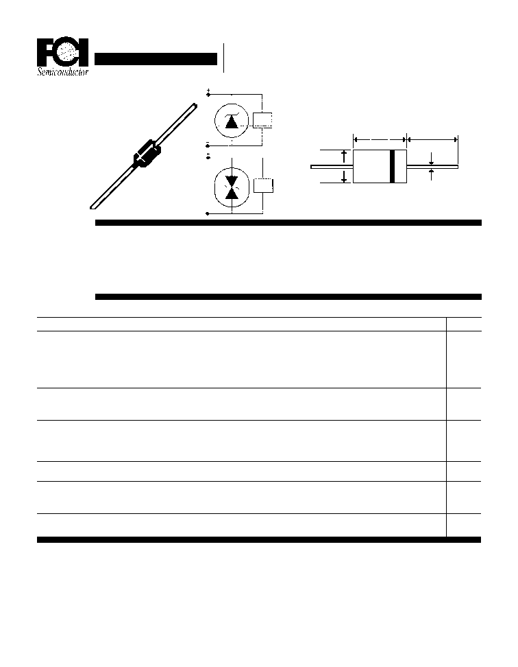
NOTES: 1. For Bi-Directional Applications, Use C or CA. Electrical Characteristics Apply in Both Directions.
2. Mounted on 20mm
2
Copper Pads.
3. 8.3 ms, ˝ Sine Wave, Single Phase Duty Cycle, @ 4 Pulses Per Minute Maximum.
4. V
BR
Measured After I
T
Applies for 300
µ
s. I
T
= Square Wave Pulse or Equivalent.
5. Non-Repetitive Current Pulse. Per Fig. 3 and Derated Above T
A
= 25
°
C Per Fig. 2.
.340
.360
1.00 Min.
.050 typ.
.340
.360
JEDEC
R6
Uni-Polar
Load
TVS
Device
TVS
Device
Load
Bi-Polar

Data Sheet
5.0V to 110V GPP TRANSIENT
VOLTAGE SUPPRESSORS
Page 11-19
Ratings at
25 Deg. C ambient
temperature
unless otherwise
specified.
Single Phase Half
Wave, 60 Hz
Resistive or
Inductive Load.
For Capacitive
Load, Derate
Current by 20%.
5KP Series
Fig. 2 Pulse Derating Curve
Ambient Temperature (
°
°
°
°
°
C)
Peak Pulse Percentage
Lead Temperature (
°
°
°
°
°
C)
Steady State Power (W)
Fig. 3 Pulse Waveform
Time (ms)
Peak Pulse Current
Fig. 6 Maximum Non-Repetitive
Surge Current
Number of Cycles @ 60 Hz
Peak Forward Surge Current (A)
20 x 20 x 1mm Cu
0
1.0
2.0
3.0
4.0
t
r
= 10
µ
s
Peak Value
I
PPM
Pulse Width is defined
as that point where the
Peak Current decays to
50% of I
PPM
5 0
100
Fig. 5 Steady State Power Derating
8.3ms Single Half Sine Wave
JEDEC Method
Fig. 1 Pulse Rating Curve
Fig. 4 Typical Junction Capacitance
Breakdown Voltage (V)
Junction Capacitance (pF)
Measured @
Standoff V
R
Measured @
Zero Bias
Non-Repetitive
Pulse Waveform
shown Fig. 3
T
A
= 25
o
C
Pulse Width
Peak Pulse Power (kW)