Äîêóìåíòàöèÿ è îïèñàíèÿ www.docs.chipfind.ru
©2004 Fairchild Semiconductor Corporation
1
www.fairchildsemi.com
May 2005
R
M
P
A
2
263
i
-
L
o
TM
W
C
D
M
A
P
o
w
e
r
A
m
pli
f
ier
Mo
du
le 19
2019
80 M
H
z
(P
r
e
l
i
m
i
n
a
r
y
)
RMPA2263
i-LoTM
Rev. G
RMPA2263
i-LoTM
WCDMA Power Amplifier Module
19201980 MHz
Features
40% WCDMA efficiency at +28 dBm Pout
14% WCDMA efficiency (85 mA total current) at +16 dBm
Pout
Linear operation in low-power mode up to +19 dBm
Low quiescent current (Iccq): 25 mA in low-power mode
Meets UMTS/WCDMA performance requirements
Meets HSDPA performance requirements
Single positive-supply operation with low power and shut-
down modes
3.4V typical Vcc operation
Low Vref (2.85V) compatible with advanced handset
chipsets
Compact Lead-free compliant LCC package
(4.0 x 4.0 x 1.5 mm nominal)
Industry standard pinout
Internally matched to 50 Ohms and DC blocked RF input/
output
General Description
The RMPA2263 Power Amplifier Module (PAM) is Fairchild's
latest innovation in 50 Ohm matched, surface mount modules
targeting UMTS/WCDMA/HSDPA applications. Answering the
call for ultra-low DC power consumption and extended battery
life in portable electronics, the RMPA2263 uses novel
proprietary circuitry to dramatically reduce amplifier current at
low to medium RF output power levels (< +16 dBm), where the
handset most often operates. A simple two-state Vmode control
is all that is needed to reduce operating current by more than
50% at 16 dBm output power, and quiescent current (Iccq) by
as much as 70% compared to traditional power-saving
methods. No additional circuitry, such as DC-to-DC converters,
are required to achieve this remarkable improvement in
amplifier efficiency. Further, the 4
x
4
x
1.5 mm LCC package is
pin-compatible and a drop-in replacement for last generation 4
x
4 mm PAMs widely used today, minimizing the design time to
apply this performance-enhancing technology. The multi-stage
GaAs Microwave Monolithic Integrated Circuit (MMIC) is
manufactured using Fairchild RF's InGaP Heterojunction
Bipolar Transistor (HBT) process.
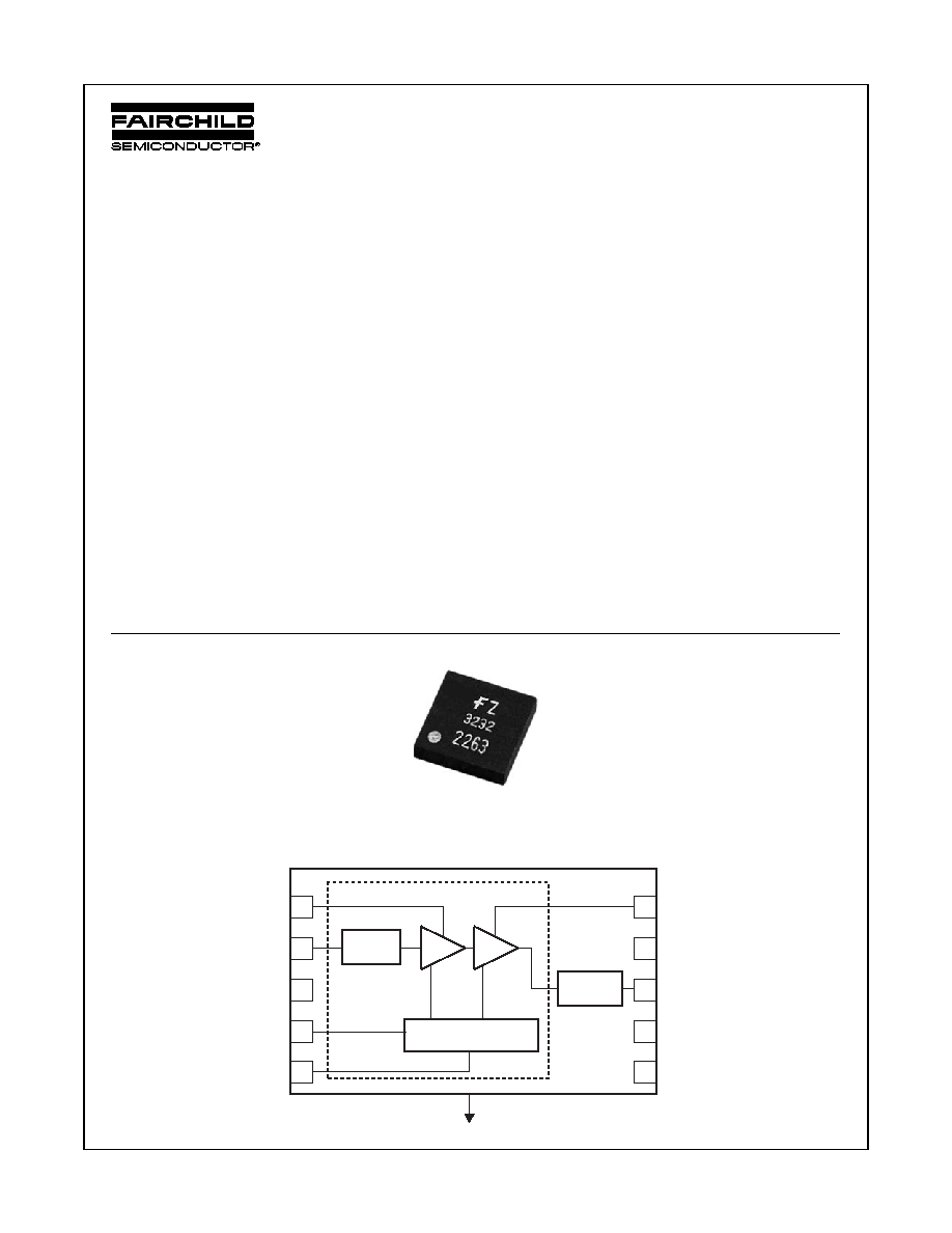
Device
Functional Block Diagram
Vref
Vmode
RF IN
GND
Vcc1
RF OUT
GND
GND
GND
7
6
8
9
10
4
3
2
BIAS/MODE SWITCH
1
5
Vcc2
11 (paddle ground on package bottom)
INPUT
MATCH
OUTPUT
MATCH
MMIC
(Top View)
PRELIMINARY
2
www.fairchildsemi.com
RMPA2263
i-LoTM
Rev. G
R
M
P
A
2
263
i
-
L
o
TM
W
C
D
M
A
P
o
we
r
A
m
plif
ier
Mo
dul
e 192
0198
0 MH
z (
P
r
e
lim
in
ar
y
)
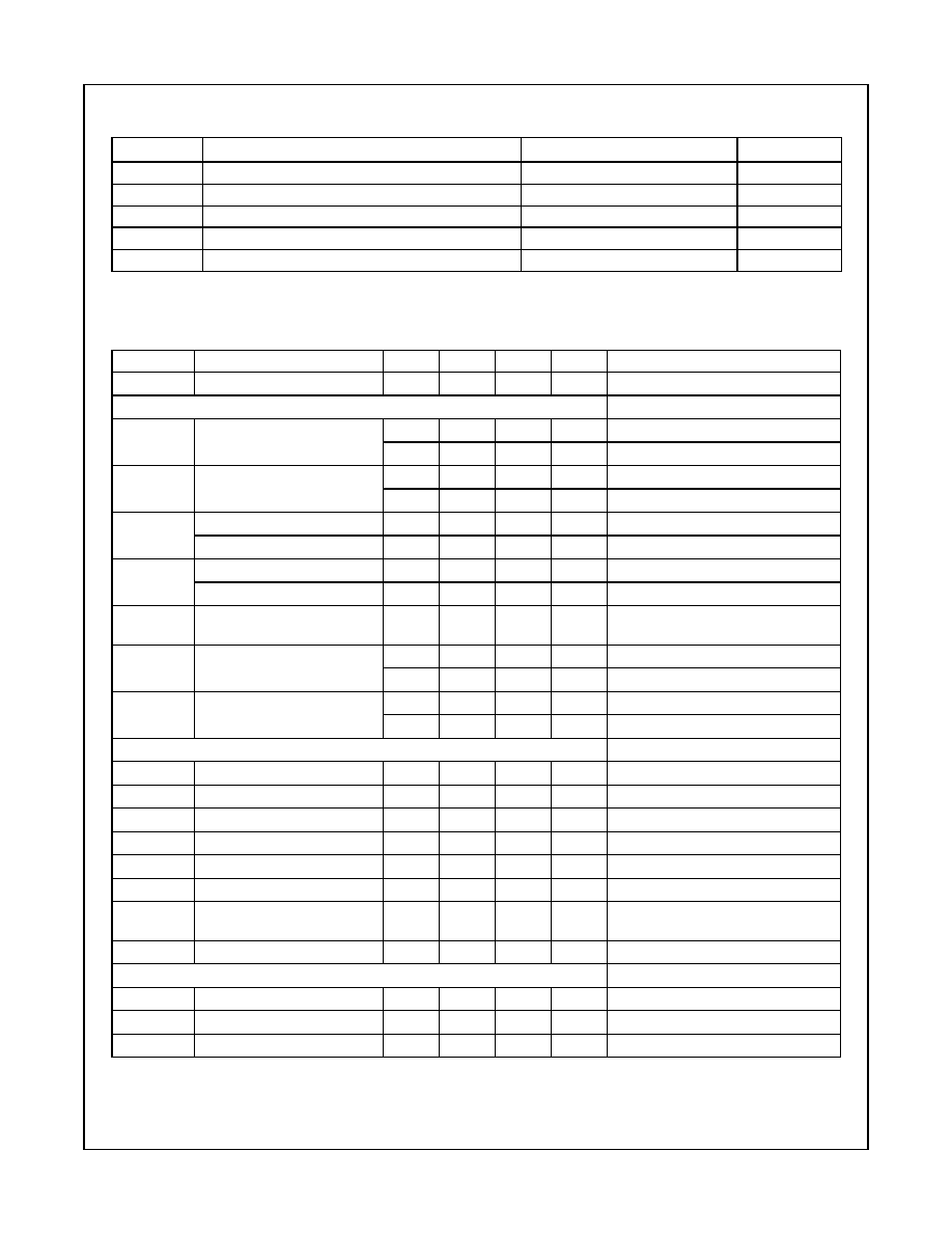
Absolute Ratings
1
Note:
1: No permanent damage with only one parameter set at extreme limit. Other parameters set to typical values.
Electrical Characteristics
1
Notes:
1. All parameters met at Tc = +25°C, Vcc = +3.4V, Vref = 2.85V and load VSWR
1.2:1, unless otherwise noted.
2. All phase angles.
3. Guaranteed by design.
Symbol
Parameter
Ratings
Units
Vcc1, Vcc2
Supply Voltages
5.0
V
Vref
Reference Voltage
2.6 to 3.5
V
Vmode
Power Control Voltage
3.5
V
Pin
RF Input Power
+10
dBm
Tstg
Storage Temperature
-55 to +150
°C
Symbol
Parameter
Min
Typ
Max
Units
Comments
f
Operating Frequency
1920
1980
MHz
WCDMA Operation
Gp
Power Gain
27.5
dB
Po=+28dBm, Vmode=0V
23
dB
Po=+16dBm, Vmode
2.0V
Po
Linear Output Power
28
dBm
Vmode=0V
16
dBm
Vmode
2.0V
PAEd
PAEd (digital) @ 28dBm
40
%
Vmode=0V
PAEd (digital) @ 16dBm
13
%
Vmode
2.0V
Itot
High Power Total Current
460
mA
Po=+28dBm, Vmode=0V
Low Power Total Current
85
mA
Po=+16dBm, Vmode
2.0V
Adjacent Channel Leakage
Ratio
WCDMA Modulation 3GPP
3.2 03-00 DPCCH+1 DCDCH
ACLR1
±5.00MHz Offset
-40
dBc
Po=+28dBm, Vmode=0V
-46
dBc
Po=+16dBm, Vmode
2.0V
ACLR2
±10.0MHz Offset
-52
dBc
Po=+28dBm, Vmode=0V
-57
dBc
Po=+16dBm, Vmode
2.0V
General Characteristics
VSWR
Input Impedance
2.0:1
2.5:1
NF
Noise Figure
4
dB
Rx No
Receive Band Noise Power
-139
dBm/Hz Po
+28dBm, 2110 to 2170 MHz
2fo
Harmonic Suppression
-38
dBc
Po
+28dBm
3fo5fo
Harmonic Suppression
-55
dBc
Po
+28dBm
S
Spurious Outputs
2, 3
-60
dBc
Load VSWR
5.0:1
Ruggedness with Load
Mismatch
3
10:1
No permanent damage
Tc
Case Operating Temperature
-30
85
°C
DC Characteristics
Iccq
Quiescent Current
25
mA
Vmode
2.0V
Iref
Reference Current
7
mA
Po
+28dBm
Icc(off)
Shutdown Leakage Current
1
5
µA
No applied RF signal
3
www.fairchildsemi.com
RMPA2263
i-LoTM
Rev. G
R
M
P
A
2
263
i
-
L
o
TM
W
C
D
M
A
P
o
we
r
A
m
plif
ier
Mo
dul
e 192
0198
0 MH
z (
P
r
e
lim
in
ar
y
)
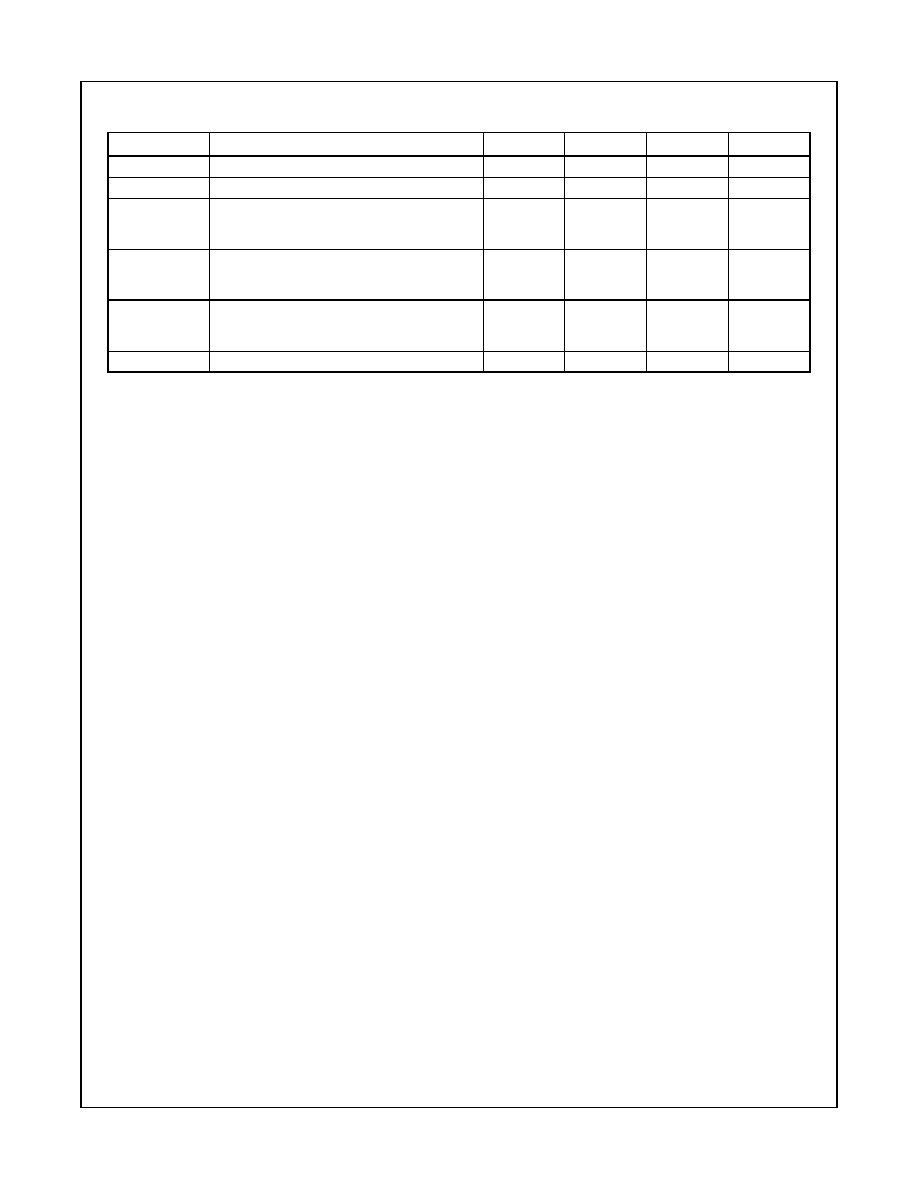
Recommended Operating Conditions
DC Turn On Sequence:
1. Vcc1 = Vcc2 = 3.4V (typical)
2. Vref = 2.85V (typical)
3. High-Power: Vmode = 0V (Pout > 16dBm)
Low-Power: Vmode = 2.0V (Pout < 16dBm)
Symbol
Parameter
Min
Typ
Max
Units
f
Operating Frequency
1920
1980
MHz
Vcc1, Vcc2
Supply Voltage
3.0
3.4
4.2
V
Vref
Reference Voltage
Operating
Shutdown
2.7
0
2.85
3.1
0.5
V
V
Vmode
Bias Control Voltage
Low-Power
High-Power
1.8
0
2.0
3.0
0.5
V
V
Pout
Linear Output Power
High-Power
Low-Power
+16
+28
+19
dBm
dBm
Tc
Case Operating Temperature
-30
+85
°C
4
www.fairchildsemi.com
RMPA2263
i-LoTM
Rev. G
R
M
P
A
2
263
i
-
L
o
TM
W
C
D
M
A
P
o
we
r
A
m
plif
ier
Mo
dul
e 192
0198
0 MH
z (
P
r
e
lim
in
ar
y
)
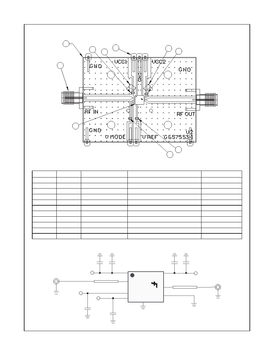
Evaluation Board Layout
Materials List
Evaluation Board Schematic
Qty
Item No.
Part Number
Description
Vendor
1
1
G657553-1 V2
PC Board
Fairchild
2
2
#142-0701-841
SMA Connector
Johnson
5
3
#2340-5211TN
Terminals
3M
Ref
4
Assembly, RMPA2263
Fairchild
3
5
GRM39X7R102K50V
1000pF Capacitor (0603)
Murata
3
5 (Alt)
ECJ-1VB1H102K
1000pF Capacitor (0603)
Panasonic
2
6
C3216X5R1A335M
3.3µF Capacitor (1206)
TDK
1
7
GRM39Y5V104Z16V
0.1µF Capacitor (0603)
Murata
1
7 (Alt)
ECJ-1VB1C104K
0.1µF Capacitor (0603)
Panasonic
A/R
8
SN63
Solder Paste
Indium Corp.
A/R
9
SN96
Solder Paste
Indium Corp.
XYTT
Z
2263
3
6
5
1
2
4
5
7
6
5
2
10
8
3, 6, 7, 9
VCC2
(PACKAGE BASE)
50 Ohm TRL
50
SMA2
RF OUT
SMA1
RF IN
Ohm TRL
3.3
µ
F
VREF
3.3
µ
F
1000 pF
1000 pF
1000 pF
0.1
µ
F
4
VMODE
11
5
VCC1
1
XYTT
Z
2263
RMPA2263
i-LoTM
Rev. G
R
M
P
A
2
263
i
-
L
o
TM
W
C
D
M
A
P
o
we
r
A
m
plif
ier
Mo
dul
e 192
0198
0 MH
z (
P
r
e
lim
in
ar
y
)
5
www.fairchildsemi.com
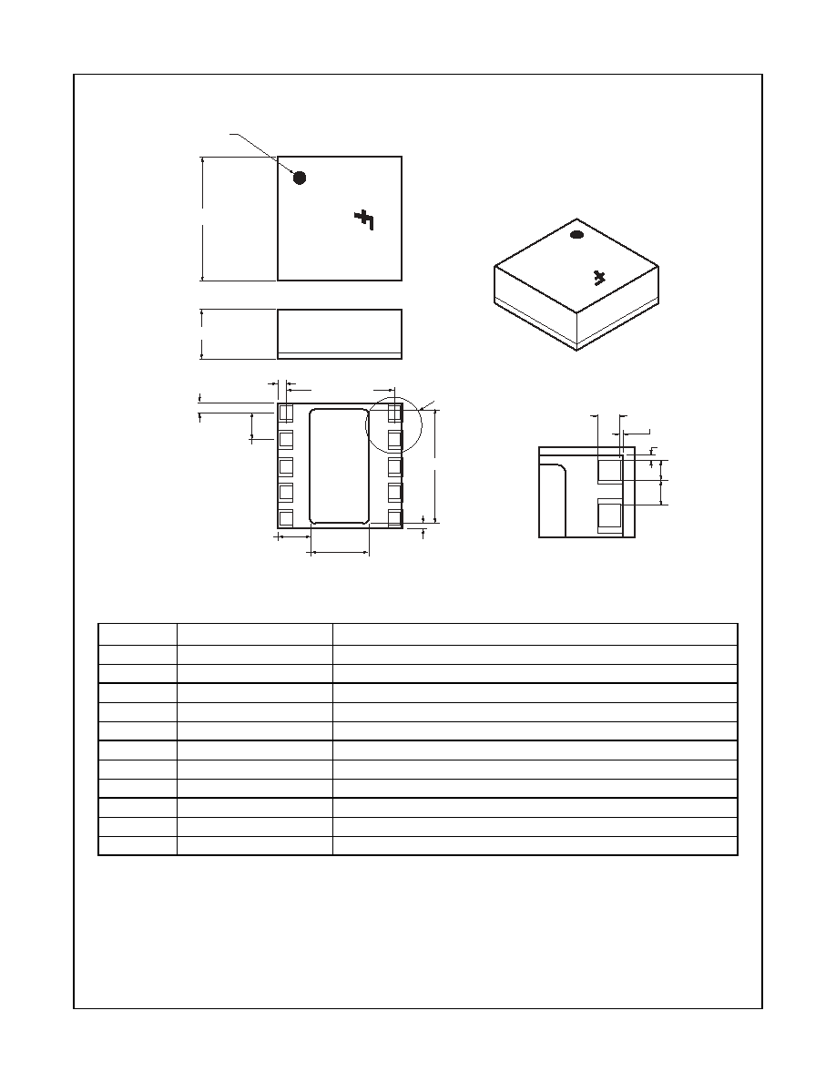
Package Outline
Signal Descriptions
Pin #
Signal Name
Description
1
Vcc1
Supply Voltage to Input Stage
2
RF In
RF Input Signal
3
GND
Ground
4
Vmode
High Power/Low Power Mode Control
5
Vref
Reference Voltage
6
GND
Ground
7
GND
Ground
8
RF Out
RF Output Signal
9
GND
Ground
10
Vcc2
Supply Voltage to Output Stage
11
GND
Paddle Ground
1
I/O 1 INDICATOR
TOP VIEW
FRONT VIEW
BOTTOM VIEW
DETAIL A. TYP.
(4.00mm
1.60mm MAX.
.30mm TYP.
.18mm
3.65mm
.85mm TYP.
.25mm TYP.
1.08mm
1.84mm
3.50mm TYP.
See Detail A
) SQUARE
+.100
.050
2
3
4
5
10
9
8
7
6
11
1
2
.40mm
.10mm
.10mm
.40mm
.45mm
XYTT
Z
2263
XYTT
Z
2263
RMPA2263
i-LoTM
Rev. G
R
M
P
A
2
263
i
-
L
o
TM
W
C
D
M
A
P
o
we
r
A
m
plif
ier
Mo
dul
e 192
0198
0 MH
z (
P
r
e
lim
in
ar
y
)
6
www.fairchildsemi.com
Applications Information
CAUTION: THIS IS AN ESD SENSITIVE DEVICE.
Precautions to Avoid Permanent Device Damage:
· Cleanliness: Observe proper handling procedures to ensure
clean devices and PCBs. Devices should remain in their
original packaging until component placement to ensure no
contamination or damage to RF, DC and ground contact
areas.
· Device Cleaning: Standard board cleaning techniques should
not present device problems provided that the boards are
properly dried to remove solvents or water residues.
· Static Sensitivity: Follow ESD precautions to protect against
ESD damage:
A properly grounded static-dissipative surface on which to
place devices.
Static-dissipative floor or mat.
A properly grounded conductive wrist strap for each person
to wear while handling devices.
· General Handling: Handle the package on the top with a
vacuum collet or along the edges with a sharp pair of bent
tweezers. Avoiding damaging the RF, DC, and ground
contacts on the package bottom. Do not apply excessive
pressure to the top of the lid.
· Device Storage: Devices are supplied in heat-sealed,
moisture-barrier bags. In this condition, devices are protected
and require no special storage conditions. Once the sealed
bag has been opened, devices should be stored in a dry
nitrogen environment.
Device Usage:
Fairchild recommends the following procedures prior to
assembly.
· Assemble the devices within 7 days of removal from the dry
pack.
· During the 7-day period, the devices must be stored in an
environment of less than 60% relative humidity and a
maximum temperature of 30°C
· If the 7-day period or the environmental conditions have been
exceeded, then the dry-bake procedure, at 125°C for 24 hours
minimum, must be performed.
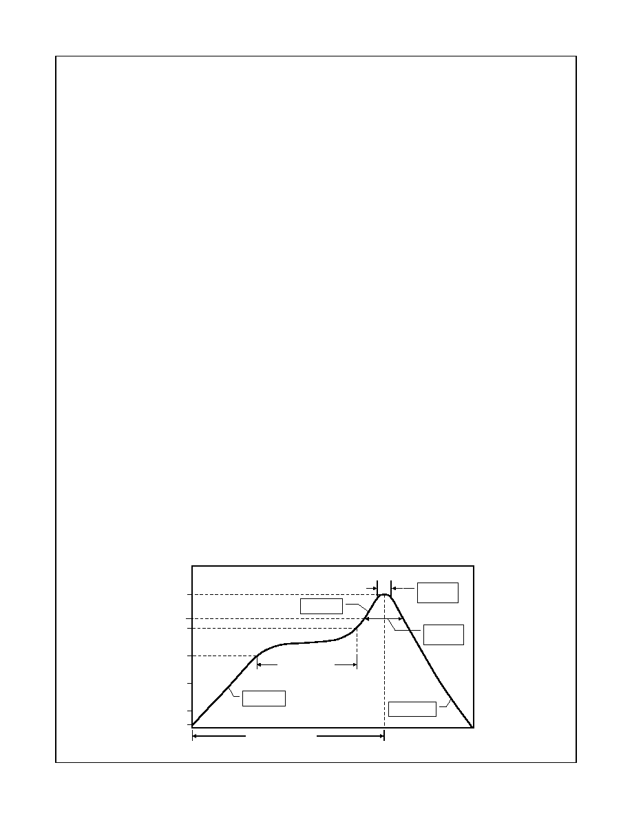
Solder Materials & Temperature Profile:
Reflow soldering is the preferred method of SMT attachment.
Hand soldering is not recommended.
Reflow Profile
· Ramp-up: During this stage the solvents are evaporated from
the solder paste. Care should be taken to prevent rapid
oxidation (or paste slump) and solder bursts caused by violent
solvent out-gassing. A maximum heating rate is 3°C/sec.
· Pre-heat/soak: The soak temperature stage serves two
purposes; the flux is activated and the board and devices
achieve a uniform temperature. The recommended soak
condition is: 60-180 seconds at 150-200°C.
· Reflow Zone: If the temperature is too high, then devices may
be damaged by mechanical stress due to thermal mismatch or
there may be problems due to excessive solder oxidation.
Excessive time at temperature can enhance the formation of
inter-metallic compounds at the lead/board interface and may
lead to early mechanical failure of the joint. Reflow must occur
prior to the flux being completely driven off. The duration of
peak reflow temperature should not exceed 20 seconds.
Soldering temperatures should be in the range 255260°C,
with a maximum limit of 260°C.
· Cooling Zone: Steep thermal gradients may give rise to
excessive thermal shock. However, rapid cooling promotes a
finer grain structure and a more crack-resistant solder joint.
The illustration below indicates the recommended soldering
profile.
Solder Joint Characteristics:
Proper operation of this device depends on a reliable void-free
attachment of the heat sink to the PWB. The solder joint should
be 95% void-free and be a consistent thickness.
Rework Considerations:
Rework of a device attached to a board is limited to reflow of the
solder with a heat gun. The device should be subjected to no
more than 15°C above the solder melting temperature for no
more than 5 seconds. No more than 2 rework operations should
be performed.
Recommended Solder Reflow Profile
150
Ramp-Up Rate
3 °C/sec max
25
Temperature (°C)
Time 25 °C/sec to peak temp
6 minutes max
Ramp-Down Rate
6 °C/sec max
Preheat, 150 to 200 °C
60 - 180 sec
200
217
Time above
liquidus temp
60 - 150 sec
100
260
Peak temp
260 +0/-5 °C
10 - 20 sec
Time (Sec)
Ramp-Up Rate
3 °C/sec max
50
7
www.fairchildsemi.com
RMPA2263
i-LoTM
Rev. G
R
M
P
A
2
263
i
-
L
o
TM
W
C
D
M
A
P
o
w
e
r
A
m
pli
f
ier
Mo
du
le 19
2019
80 M
H
z
(P
r
e
l
i
m
i
n
a
r
y
)
DISCLAIMER
FAIRCHILD SEMICONDUCTOR RESERVES THE RIGHT TO MAKE CHANGES WITHOUT FURTHER NOTICE TO ANY
PRODUCTS HEREIN TO IMPROVE RELIABILITY, FUNCTION OR DESIGN. FAIRCHILD DOES NOT ASSUME ANY LIABILITY
ARISING OUT OF THE APPLICATION OR USE OF ANY PRODUCT OR CIRCUIT DESCRIBED HEREIN; NEITHER DOES IT
CONVEY ANY LICENSE UNDER ITS PATENT RIGHTS, NOR THE RIGHTS OF OTHERS.
TRADEMARKS
The following are registered and unregistered trademarks Fairchild Semiconductor owns or is authorized to use and is
not intended to be an exhaustive list of all such trademarks.
LIFE SUPPORT POLICY
FAIRCHILD'S PRODUCTS ARE NOT AUTHORIZED FOR USE AS CRITICAL COMPONENTS IN LIFE SUPPORT
DEVICES OR SYSTEMS WITHOUT THE EXPRESS WRITTEN APPROVAL OF FAIRCHILD SEMICONDUCTOR CORPORATION.
As used herein:
1. Life support devices or systems are devices or
systems which, (a) are intended for surgical implant into
the body, or (b) support or sustain life, or (c) whose
failure to perform when properly used in accordance
with instructions for use provided in the labeling, can be
reasonably expected to result in significant injury to the
user.
2. A critical component is any component of a life
support device or system whose failure to perform can
be reasonably expected to cause the failure of the life
support device or system, or to affect its safety or
effectiveness.
PRODUCT STATUS DEFINITIONS
Definition of Terms
Datasheet Identification
Product Status
Definition
Advance Information
Preliminary
No Identification Needed
Obsolete
This datasheet contains the design specifications for
product development. Specifications may change in
any manner without notice.
This datasheet contains preliminary data, and
supplementary data will be published at a later date.
Fairchild Semiconductor reserves the right to make
changes at any time without notice in order to improve
design.
This datasheet contains final specifications. Fairchild
Semiconductor reserves the right to make changes at
any time without notice in order to improve design.
This datasheet contains specifications on a product
that has been discontinued by Fairchild semiconductor.
The datasheet is printed for reference information only.
Formative or
In Design
First Production
Full Production
Not In Production
IntelliMAXTM
ISOPLANARTM
LittleFETTM
MICROCOUPLERTM
MicroFETTM
MicroPakTM
MICROWIRETM
MSXTM
MSXProTM
OCXTM
OCXProTM
OPTOLOGIC
OPTOPLANARTM
PACMANTM
FAST
FASTrTM
FPSTM
FRFETTM
GlobalOptoisolatorTM
GTOTM
HiSeCTM
I
2
CTM
i-LoTM
ImpliedDisconnectTM
Rev. I15
ACExTM
ActiveArrayTM
BottomlessTM
CoolFETTM
CROSSVOLTTM
DOMETM
EcoSPARKTM
E
2
CMOSTM
EnSignaTM
FACTTM
FACT Quiet SeriesTM
POPTM
Power247TM
PowerEdgeTM
PowerSaverTM
PowerTrench
QFET
QSTM
QT OptoelectronicsTM
Quiet SeriesTM
RapidConfigureTM
RapidConnectTM
µ
SerDesTM
SILENT SWITCHER
SMART STARTTM
SPMTM
StealthTM
SuperFETTM
SuperSOTTM-3
SuperSOTTM-6
SuperSOTTM-8
SyncFETTM
TinyLogic
TINYOPTOTM
TruTranslationTM
UHCTM
UltraFET
UniFETTM
VCXTM
Across the board. Around the world.TM
The Power Franchise
Programmable Active DroopTM
Document Outline