Electronics
Semiconductor Division
Features
· Triple video amplifier with internal resistors to set gains to
+2, +1, and -1
· Independently enabled amplifiers
· 60 MHz -3 dB Bandwidth (A
V
= 2)
· 20 MHz
±
0.1 dB gain flatness
· 0.06% differential gain (A
V
= 2, R
L
= 150
)
· 0.06
°
differential phase (A
V
= 2, R
L
= 150
)
· High CMRR (75 dB), High PSRR (70 dB)
· Dual
±
5V power supply
· Low offset 2.0 mV
· 16-pin narrow SOIC package
· 300 V/
µ
s slew rate
· Fast settling time: 0.1% in 35 ns
· Voltage gain accuracy better than 0.5%
· TTL or CMOS compatible enable inputs
Applications
· RGB amplifier
· 3:1 crosspoint switch
· RGB switch
· Video instrumentation amplifier
· Selectable gain amplifier
· Programmable filter
· Active filter
Description
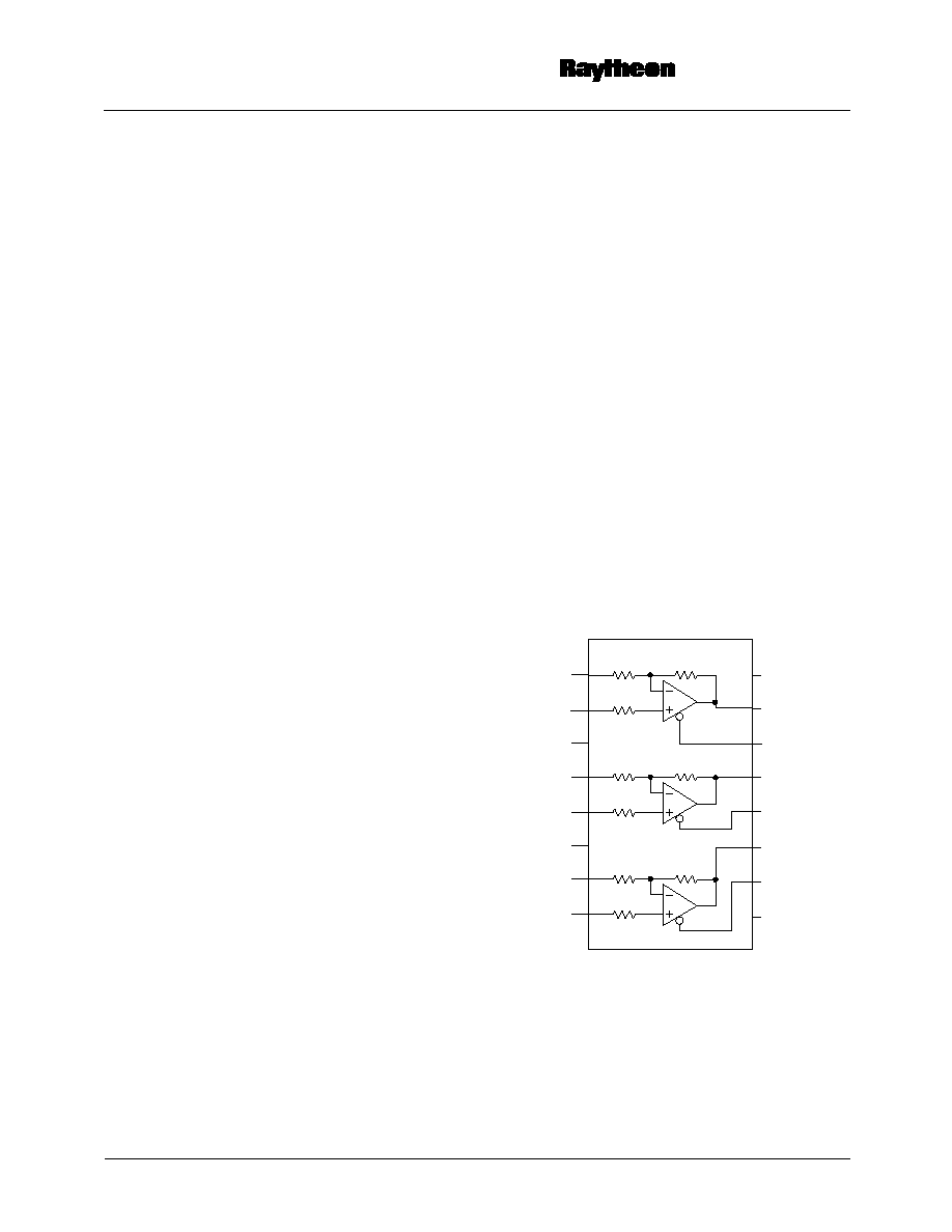
The RC6704 consists of three low power, wide band voltage
feedback operational amplifiers. Internal thin-film gain set-
ting resistors provide gains of +2, +1 and -1. Each channel is
capable of delivering a load current of at least 35mA.
Each amplifier can be independently enabled or disabled
with a TTL or CMOS signal. When disabled, the amplifier is
in a high impedance output state, presenting a very high
input to output isolation. The layout is optimized for low
channel to channel crosstalk.
The amplifiers are optimized for video applications where
low differential gain and low phase distortion are significant
requirements.
Block Diagram
65-7450
V
CCO
OUT1
EN1
OUT2
EN2
OUT3
EN3
V
EEO
IN1
IN1+
V
CC
IN2
IN2+
V
EE
IN3
IN3+
R
R
R/2
R
R
R/2
R
R
R/2
R = 500
RC6704
Triple Fixed Gain Video Amplifier
with Separate Enable Inputs
Rev. 1.0.1
RC6704
PRODUCT SPECIFICATION
2
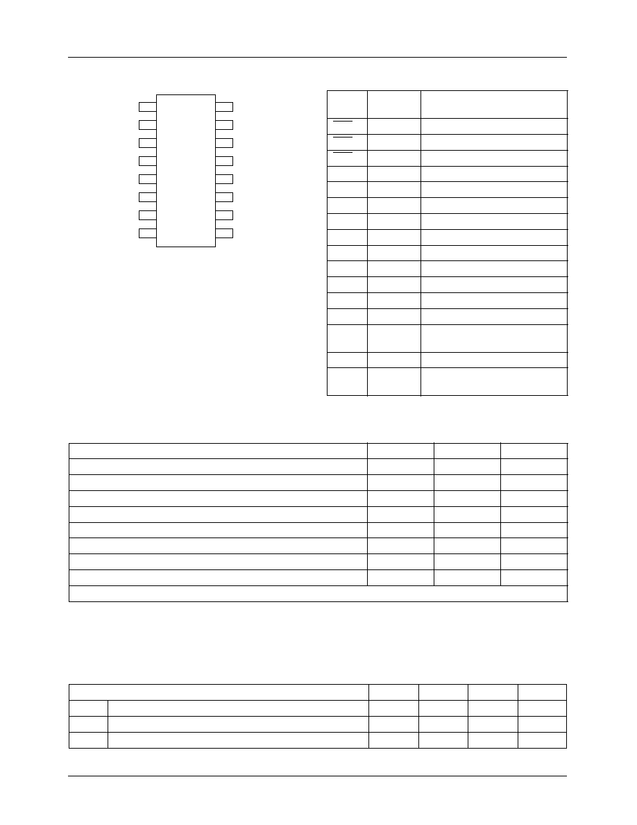
Pin Assignments
16
15
14
13
12
11
10
9
65-3399-03
V
CCO
OUT1
EN1
OUT2
EN2
OUT3
EN3
VEEO
1
2
3
4
5
6
7
8
IN1
IN1+
V
CC
IN2
IN2+
V
EE
IN3
IN3+
Pin Definitions
Pin
Name
Pin
Number
Pin Function Description
EN1
14
Enables amplifier 1 when low
EN2
12
Enables amplifier 2 when low
EN3
10
Enables amplifier 3 when low
IN1
1
Amplifier 1 inverting input
IN1+
2
Amplifier 1 non-inverting input
IN2
4
Amplifier 2 inverting input
IN2+
5
Amplifier 2 non-inverting input
IN3
7
Amplifier 3 inverting input
IN3+
8
Amplifier 3 non-inverting input
OUT1
15
Amplifier 1 output
OUT2
13
Amplifier 2 output
OUT3
11
Amplifier 3 output
V
CC
3
Analog positive supply
V
CCO
16
Positive supply for output
stages
V
EE
6
Analog negative supply
V
EEO
9
Negative supply for output
stages
Absolute Maximum Ratings
(beyond which the device may be damaged)1
Note:
1. Functional operation under any of these conditions is NOT implied. Performance and reliability are guaranteed only if
Operating Conditions are not exceeded.
Operating Conditions
Parameter
Min.
Max.
Units
Positive power supply, V
CC
7
V
Negative power supply, V
EE
-7
V
Differential input voltage
V
EE
+ 2.0
V
CC
2.0
V
Operating Temperature
0
+70
°
C
Storage Temperature
-40
+125
°
C
Junction Temperature
150
°
C
Lead Soldering Temperature (10 seconds)
300
°
C
Operating Temperature
0
+70
°
C
Short circuit tolerance: No more than one output can be shorted to ground.
Parameter
Min.
Typ.
Max.
Units
V
CC
Power Supply Voltage
4.75
5.0
5.25
V
V
EE
Negative Supply Voltage
-4.75
-5.0
-5.25
V
JA
SO16 thermal resistance
105
°
C/W
PRODUCT SPECIFICATION
RC6704
3
DC Characteristics
V
CC
= 5V, V
EE
= -5V, A
V
= 2, R
LOAD
= 150
, T
A
= 0
°
C to 70
°
C, unless otherwise specified.
Note:
1. Guaranteed by design.
Parameter
Conditions
Min.
Typ.
Max.
Units
V
OS
Input Offset Voltage
No Load
±
2
±
5
mV
V
OS
/
T Offset Voltage Drift
1
±
12
±
50
µ
V/
°
C
I
B
Input Bias Current
±
2
±
10
µ
A
I
B
/
T
Input Bias Current Drift
1
±
10
±
50
nA/
°
C
Rin
Input Resistance
1
1
M
Cin
Input Capacitance
1
0.5
2
pF
CMIR
Common Mode Input Range
±
2.5
V
CMRR
Common Mode Rejection Ratio No Load
60
75
dB
PSRR
Power Supply Rejection Ratio
No Load
60
70
dB
Is
Quiescent Supply Current
No Load, Whole IC
25
35
mA
Isd
Supply Current Disabled
3
4
mA
R
OUT
Output Impedance
1
Enabled, at DC
0.2
C
OUT
Output Capacitance
1
Disabled
0.5
pF
I
OUT
Output Current
35
mA
V
OUT
Output Voltage Swing
No Load
±
2.5
±
3.0
V
R
L
= 150
±
2.5
±
3.0
V
A
V
Closed-loop Gain
1.99
2.0
2.01
dB
A
V
/
T
Closed-loop Gain Drift
1
25
ppm/
°
C
Venh
Enable High Voltage
2.4
V
Venl
Enable Low Voltage
0.8
V
Ien
Enable Input Current
3
10
µ
A
t
off
Disable Time
1
1.0
ns
t
on
Enable Time
1
Settling to 1%
200
ns

RC6704
PRODUCT SPECIFICATION
4
AC Characteristics
V
CC
= 5V, V
EE
= -5V, A
V
= 2, T
A
= 0 to 70
°
C, R
LOAD
= 150
, C
L
= 10 pF unless otherwise specified.
Note:
1. Guaranteed by design.
Test Circuits
Note:
1. When driving a 75
cable, the source terminator resistor must be placed as close as possible to the output of the device.
Parameter
Conditions
Min.
Typ.
Max.
Units
Frequency Response
BW
-3 dB Bandwidth (A
V
= 2)
1
V
OUT
= 0.4 Vpp
60
MHz
V
OUT
= 0.8 Vpp
55
MHz
Flat
±
0.1 dB Bandwidth
1
15
20
MHz
Peak
Maximum Small Signal AC
Peaking
1
0.4
0.7
dB
ISO
Off Isolation
1
@ 5 MHz
90
dB
X
TALK
Crosstalk Isolation
1
@ 5 MHz, R
IN
= 50
70
dB
Time Domain Response
t
r1
, t
f1
Rise and Fall Time 10% to 90%
1
2V Output Step
7
10
ns
ts
Settling time to 0.1 %
1
2V Output Step
35
ns
OS
Overshoot
1
2V Output Step
6
%
US
Undershoot
1
2V Output Step
1.5
%
SR
Slew Rate
1
V
OUT
=
±
2.0V
200
300
V/
µ
s
Distortion
HD
2
2nd Harmonic Distortion
1
V
OUT
= 0.8 Vpp, @ FO = 20
MHz
-50
dB
HD
3
3nd Harmonic Distortion
1
V
OUT
= 0.8 Vpp, @ FO = 20
MHz
-50
dB
Equivalent Input Noise
NF
Noise Floor > 100 KHz
1
-140
dBm
SND
Spectral Noise Density
1
100 kHz to 200 MHz
10
nV/
Hz
Video Performance
DG
Diff. Gain (p-p), NTSC & PAL
1
R
L
= 150
, V
OUT
=
±
1.5V
0.06
%
DP
Diff. Phase (p-p), NTSC & PAL
1
R
L
= 150
, V
OUT
=
±
1.5V
0.06
Deg.
1/3
RC6704
10 pF
C
L
75
R
L
75
Video
Output
Video
Input
R
S
R
LOAD
= R
L
+ R
S
A
V
= +2
A
V
= +1
A
V
= -1
1/3
RC6704
10 pF
C
L
75
R
L
75
Video
Output
Video
Input
R
S
R
LOAD
= R
L
+ R
S
R
LOAD
= R
L
+ R
S
1/3
RC6704
10 pF
C
L
75
R
L
75
Video
Output
Video
Input
R
S
65-7479
PRODUCT SPECIFICATION
RC6704
5
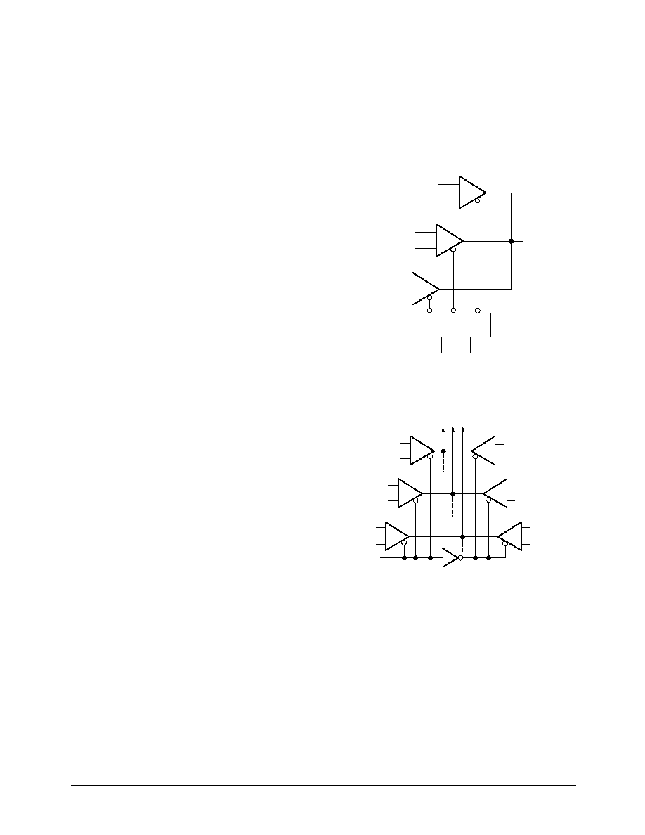
Applications Discussion
Each of the three sections of the RC6704 is provided with an
Enable input, thus the part is useful for selecting and multi-
plexing. It is suitable for selectable gain and programmable
filter applications. A three-channel video multiplexer can be
built with just one RC6704 and a decoder, as shown in
Figure 1.
Note that RC6704 enable time is shorter than its disable
time, hence a make-before-break action is provided, mini-
mizing switching transients on the signal output.
An RGB switch is shown in Figure 2.
Capacitive Load
The RC6704 can drive a capacitive load from 10 to over 100
pF. In back terminated video applications, bandwidth will
only be limited by the RC time constants of the external out-
put components. A minimum 10 pF capacitive load is
required. When driving a 75
cable, place the 75
source
termination resistor as close to the amplifier output as possi-
ble.
Enable/Disable
The enable pins (10, 12, 14), when pulled to a TTL or
CMOS logic low or when tied to ground, activate each
amplifier individually. When pulled to a TTL or CMOS logic
high, the amplifier is tri-stated and presents a high imped-
ance at its output. When disabled the amplifier's power con-
sumption drops, and the non-inverting input signal is isolated
from its respective output.
DC Accuracy
The RC6704 is a voltage-feedback amplifier; the inverting
and non-inverting inputs have similar impedances and bias
currents. To minimize offset voltage, the resistances seen by
inverting and non-inverting inputs must be equal.
Circuit Board
High-frequency applications require good grounding, power
supply decoupling, low parasitic capacitance and inductance,
and good isolation between the inputs to minimize crosstalk.
Avoid coupling from output to input to prevent positive feed-
back.
Figure 1.
Figure 2.
Decoder
+
+
+
Output
Channel 1
Input
65-7460
Channel 2
Input
Channel 3
Input
R
G
B
+
+
+
R
G
B
Channel b
Red Input
Channel b
Green Input
Channel b
Blue Input
+
+
+
Channel a
Red Input
Channel a
Green Input
Channel a
Blue Input
R
G
B
Channel
Select
R G
Video Busses
74LS04
65-7461
B