Äîêóìåíòàöèÿ è îïèñàíèÿ www.docs.chipfind.ru
PRELIMINARY INFORMATION describes products that are not in full production at the time of printing. Specifications are based on design goals
and limited characterization. They may change without notice. Contact Raytheon for current information.
www.fairchildsemi.com
REV. 1.0.1 4/8/02
Features
· High accuracy output voltage
· Guaranteed 100 mA output current
· Extremely low quiescent current
· Extremely tight load and line regulation
· Requires only a 1.0µF output capacitor for stability
· Internal Current and Thermal Limiting
· Error flag warns of output dropout
· Logic-controlled electronic shutdown
· Output programmable from 1.24 to 29V
· Fixed 3.3V version available
· -25°C to +85°C operating range
· 8 lead SOIC package
Description
The RC2951 is a voltage regulator specifically designed to
maintain proper regulation with a very low dropout voltage
(Typ. 40mV at light loads and 380 mV at 100mA). It has a
low quiescent bias current of 75
µA and is capable of supply-
ing output currents in excess of 100mA. It has internal cur-
rent and thermal limiting protection. The output can be
programmed from 1.24V to 29V with two external resistors.
A fixed output voltage (3.3V) is also available.
The error flag output can be used as power-on reset for
warning of a low output voltage. The Shutdown input feature
allows a logic level signal to turn on and off the regulator
output. The RC2951 is ideally suited for battery powered
computer, consumer, and industrial equipment where an
extension of useful battery life is desirable. The RC2951 is
available in an 8-pin SOIC package.
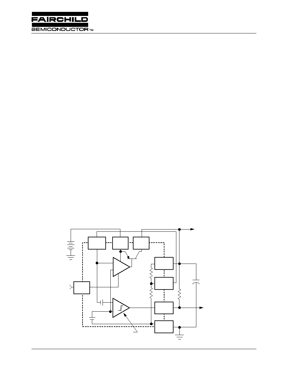
Block Diagram
Unregulated DC
+
Shut
Down
Feed-
Back
Error
Amplifier
1.23V
Reference
From
CMOS
or TTL
To CMOS
or TTL
Input
Output
Sense
330k
60 mV
3
7
8
1
2
6
5
4
V
TAP
I
L
100 mA
V
OUT
See Application
Discussion
Error Detection Comparator
Ground
Error
+
+
+
+
+
RC2951
Adjustable Micropower Voltage Regulator
RC2951
PRODUCT SPECIFICATION
2
REV. 1.0.1 4/8/02
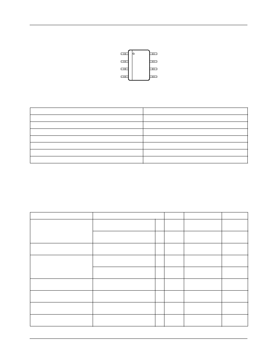
Pin Assignments
Absolute Maximum Ratings
Notes:
1. Junction to ambient thermal resistance for the S.O. (M) package is 160
°C/W.
2
May exceed input supply voltage.
3. When used in dual-supply systems where the output terminal sees loads returned to a negative supply, the output voltage
should be diode-clamped to ground.
Power Dissipation
Internally Limited
Lead Temp. (Soldering, 5 seconds)
260
°C
Storage Temperature Range
65
° to +150°C
Operating Junction Temperature Range
1
55
° to +150°C
Input Supply/Voltage
0.3 to +30V
Feedback Input Voltage
2,3
1.5 to +30V
Shutdown Input Voltage
2
0.3 to +30V
Error Comparator Output Voltage
2
0.3 to +30V
Electrical Characteristics
The
· denotes that the limits apply at temperature extremes.
Parameter
Conditions
1
Typ.
Tested Limit
2
Units
Output Voltage
(RC2951M)
T
J
= 25
°C
5.0
5.025
4.975
V max
V min
-25
°C T
J
85°C
·
·
5.0
5.06
4.94
V max
V min
Output Voltage
(RC2951M)
100
µA I
L
100mA
T
J
T
JMAX
·
·
5.0
5.075
4.925
V max
V min
Output Voltage
(RC2951M-3.3)
T
J
= 25
°C
3.3
3.317
3.284
V max
V min
-25
°C T
J
85°C
·
·
3.3
3.340
3.260
V max
V min
Output Voltage
(RC2951M-3.3)
100
µA I
L
100mA
T
J
T
JMAX
·
·
3.3
3.346
3.254
V max
V min
Output Voltage Temperature
Coefficient
7
·
20
120
ppm/
°C
Line Regulation
9, 10
(V
O
NOM + 1)V
V
in
20V
·
0.03
0.1
0.5
% max
% max
Load Regulation
9
100
µA I
L
100 mA
·
0.08
0.2
0.4
% max
% max
Output
Sense
Shutdown
Ground
Input
8
7
6
5
1
2
3
4
Feedback
V
TAP
Error
Top View
8 Lead SOIC Package
PRODUCT SPECIFICATION
RC2951
REV. 1.0.1 4/8/02
3
Dropout Voltage
3
I
L
= 100
µA
·
50
80
150
mV max
mV max
I
L
= 100 mA
·
380
500
700
mV max
mV max
Ground Current
I
L
= 100
µA
·
75
120
140
µA max
µA max
I
L
= 100 mA
·
8
14
15
mA max
mA max
Dropout Ground Current
V
in
= (V
O
NOM - 0.5)V
I
L
= 100
µA
·
110
250
300
µA max
µA max
Current Limit
V
out
= 0
·
160
200
220
mA max
mA max
Thermal Regulation
8
0.05
0.2
%/W max
Output Noise,
10 Hz to
100 KHz
C
L
= 1
µF (5V Only)
430
µV rms
C
L
= 200
µF
160
µV rms
C
L
= 3.3
µF
(Bypass = 0.01
µF
Pins 7 to 1 (RC2951)
100
µV rms
Reference Voltage
·
·
1.235
1.25
1.26
1.22
1.2
V max
V max
V min
V min
Reference Voltage
5
·
·
1.27
1.19
V max
V min
Feedback Pin Bias Current
·
20
40
60
nA max
nA max
Reference Voltage
Temperature Coefficient
7
20
ppm/
°C
Feedback Pin Bias Current
Temperature Coefficient
0.1
nA/
°C
Error Comparator
Output Leakage Current
V
OH
= 30V
·
0.01
1
2
µA max
µA max
Output Low Voltage
V
in
= (V
O
NOM - 0.5)V
I
OL
= 400
µA
·
150
250
400
mV max
mV max
Upper Threshold Voltage
4
·
60
40
25
mV min
mV min
Lower Threshold Voltage
4
·
75
95
140
mV max
mV max
Hysteresis
4
15
mV
Electrical Characteristics
(continued)
The
· denotes that the limits apply at temperature extremes.
Parameter
Conditions
1
Typ.
Tested Limit
2
Units
RC2951
PRODUCT SPECIFICATION
4
REV. 1.0.1 4/8/02
Notes:
1. Unless otherwise specified all limits guaranteed for T
J
= 25
°C, V
in
= (V
O
NOM + 1)V, I
L
= 100
µA and C
L
= 1
µF for 5V
versions, and 2.2
µF for 3V and 3.3V versions. Additional conditions for the 8-pin versions are Feedback tied to V
TAP
,
Output tied to Output Sense and V
shutdown
< 0.8V.
2. Guaranteed and 100% production tested.
3. Dropout Voltage is defined as the input to output differential at which the output voltage drops 100 mV below its nominal value
measured at 1V differential. At very low values of programmed output voltage, the minimum input supply voltage of 2V (2.3V
over temperature) must be taken into account.
4. Comparator thresholds are expressed in terms of a voltage differential at the Feedback terminal below the nominal
reference voltage measured at V
in
= (V
O
NOM + 1)V. To express these thresholds in terms of output voltage change, multiply
by the error amplifier gain = V
out
/V
ref
= (R1 + R2)/R2. For example, at a programmed output voltage of 5V, the Error output
is guaranteed to go low when the output drops by 95 mV x 5V/1.235V = 384 mV. Thresholds remain constant as a percent
of V
out
as V
out
is varied, with the dropout warning occurring at typically 5% below nominal, 7.5% guaranteed.
5. V
ref
< V
out
(V
in
1V), 2.3V
V
in
30V, 100µA I
L
100 mA, T
J
T
JMAX
.
6. V
shutdown
2V, V
in
30V, V
out
= 0, Feedback pin tied to V
TAP
.
7. Output or reference voltage temperature coefficient is defined as the worst case voltage change divided by the total
temperature range.
8. Thermal regulation is defined as the change in output voltage at a time T after a change in power dissipation is applied,
excluding load or line regulation effects. Specifications are for a 50 mA load pulse at V
IN
= 30V (1.25W pulse) for
T = 10 ms.
9. Regulation is measured at constant junction temperature, using pulse testing with a low duty cycle. Changes in output voltage
due to heating effects are covered under the specification for thermal regulation.
10. Line regulation for the RC2951 is tested at 150
°C for I
L
= 1 mA. For I
L
= 100
µA and T
J
= 125
°C, line regulation is guaranteed
by design to 0.2%. See Typical Performance Characteristics for line regulation versus temperature and load current.
Shutdown Input
Input Logic Voltage
Low (Regulator ON)
High (Regulator OFF)
·
·
1.3
0.6
2.0
V
V max
V min
Shutdown Pin Input Current
V
shutdown
= 2.4V
·
30
50
100
µA max
µA max
V
shutdown
= 30V
·
450
600
750
µA max
µA max
Regulator Output
Current in Shutdown
6
·
3
10
20
µA max
µA max
Electrical Characteristics
(continued)
The
· denotes that the limits apply at temperature extremes.
Parameter
Conditions
1
Typ.
Tested Limit
2
Units
PRODUCT SPECIFICATION
RC2951
REV. 1.0.1 4/8/02
5
Applications Discussion
The RC2951 regulator is designed with internal current lim-
iting and thermal shutdown. It is not internally compensated
and requires a 1.0µF (or greater) capacitor between the out-
put terminal and ground for stability. At lower output volt-
ages, more capacitance is required (2.2µF or more is
recommended for 3V and 3.3V versions) for stability. Most
types of aluminum, tantalum or multilayer ceramic capaci-
tors will perform adequately. Solid tantalums or appropriate
multilayer ceramic capacitors are suggested for operation
below 25°C. At lower values of output current, less capaci-
tance is needed to maintain stability at output. The capacitor
at the output can be reduced to 0.33µF for currents less that
10mA, or 0.1µF for currents below 1.0mA.
Using the adjustable versions at voltages below 5V runs the
error amplifier at lower gains so that more output capaci-
tance is needed. For the worst-case situation of a 100 mA
load at 1.23V output (Output shorted to Feedback) a
3.3
µF (or greater) capacitor should be used.
When setting the output voltage of the RC2951 versions with
external resistors, a minimum load of 1
µA is recommended.
A 1
µF tantalum or aluminum electrolytic capacitor should
be placed from the RC2951 input to ground if there is more
than 10 inches of wire between the input and the AC filter
capacitor or if a battery is used as the input.
Stray capacitance to the RC2951 Feedback terminal can
cause instability. This may especially be a problem when
using high value external resistors to set the output voltage.
Adding a 100 pF capacitor between Output and Feedback
and increasing the output capacitor to at least 3.3
µF will fix
this problem.
Error Detection Comparator Output
The comparator switches to a logic low whenever the
RC2951 output falls out of regulation by more than approxi-
mately 5%. This value is the comparator's built-in offset of
about 60 mV divided by the 1.235 internal reference voltage.
This trip level remains "5% below normal" regardless of the
value of the output voltage. For example, the error flag trip
level is typically 4.75V for a 5V output or 11.4V for a 12V
output. The out of regulation condition may be due either to
low input voltage, current limiting, or thermal limiting.
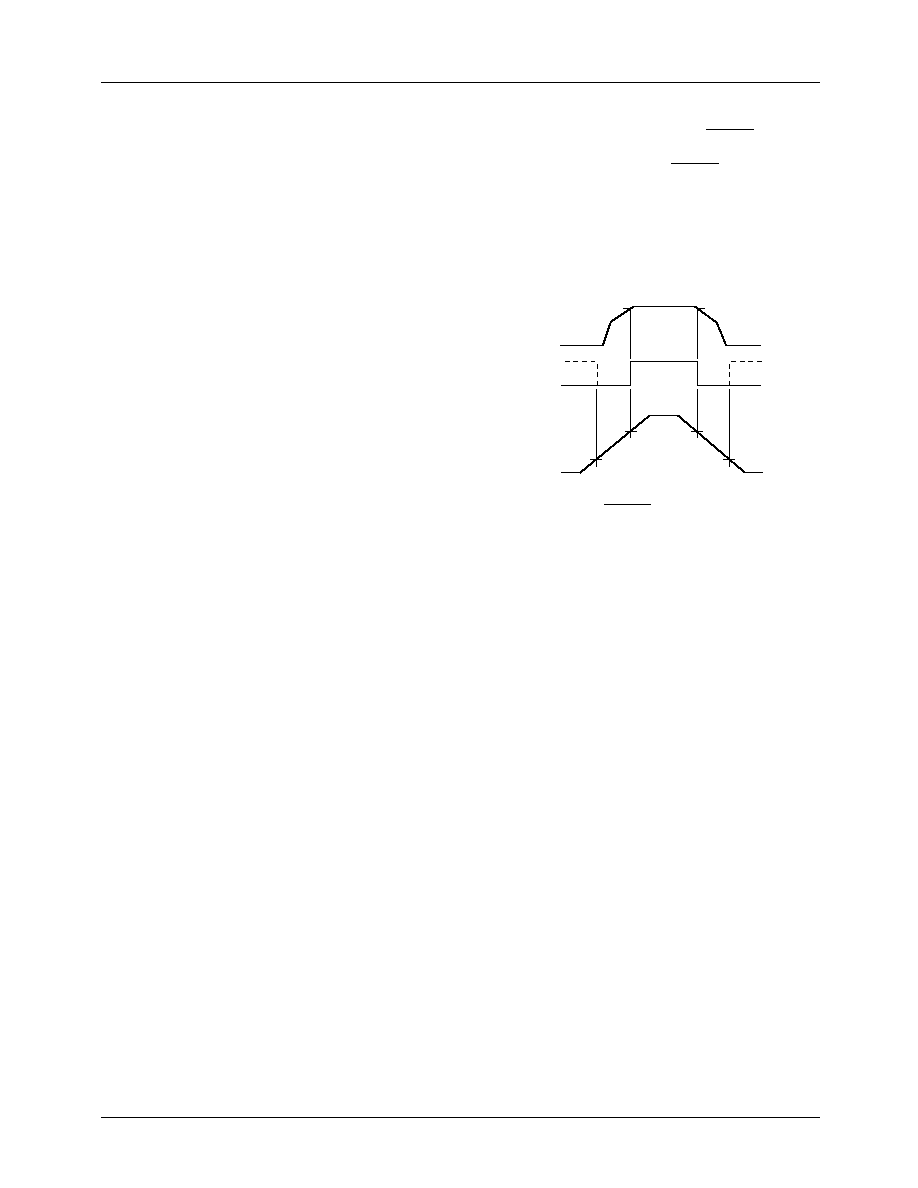
Figure 1 is a timing diagram showing the ERROR signal and
the regulated output voltage as the RC2951 input is ramped
up and down. For 5V versions, the ERROR signal becomes
valid (low) at about 1.3V input. It goes high at about 5V
input (the input voltage at which V
OUT
= 4.75.) Since the
RC2951's dropout voltage is load-dependent (see curve in
typical performance characteristics), the input voltage trip
point (about 5V) will vary with the load current. The output
voltage trip point (approx. 4.75V) does not vary with load.
Figure 1. ERROR Output Timing
The error comparator has an open-collector output which
requires an external pullup resistor. This resistor may be
returned to the output or some other supply voltage depend-
ing on system requirements. In determining a value for this
resistor, note that while the output is rated to sink 400
µA,
this sink current adds to battery drain in a low battery condi-
tion. Suggested values range from 100k to 1M
. The resistor
is not required if this output is unused.
Programming the Output Voltage (RC2951)
The RC2951 may be pin-strapped for the nominal fixed
output voltage using its internal voltage divider by tying the
output and sense pins together, and also tying the feedback
and V
TAP
pins together. Alternatively, it may be programmed
for any output voltage between its 1.235V reference and its
30V maximum rating. As seen in Figure 2 an external pair of
resistors is required.
Output
Voltage
Input
Voltage
5V
1.3V
4.75V
2950-10
Error*