Äîêóìåíòàöèÿ è îïèñàíèÿ www.docs.chipfind.ru
PN5432 / PN5433 / PN5434
PN5432
PN5433
PN5434
N-Channel Switch
This device is designed for analog or digital switching applications where
very low On Resistance is mandatory. Sourced from Process 58. See
J108 for characteristics.
Absolute Maximum Ratings*
TA = 25°C unless otherwise noted
*
These ratings are limiting values above which the serviceability of any semiconductor device may be impaired.
NOTES:
1) These ratings are based on a maximum junction temperature of 150 degrees C.
2) These are steady state limits. The factory should be consulted on applications involving pulsed or low duty cycle operations.
Thermal Characteristics
TA = 25°C unless otherwise noted
Symbol
Parameter
Value
Units
V
DG
Drain-Gate Voltage
25
V
V
GS
Gate-Source Voltage
-25
V
I
GF
Forward Gate Current
10
mA
T
J
, T
stg
Operating and Storage Junction Temperature Range
-55 to +150
°
C
Symbol
Characteristic
Max
Units
PN5432 / 5433 / 5434
P
D
Total Device Dissipation
Derate above 25
°
C
350
2.8
mW
mW/
°
C
R
JC
Thermal Resistance, Junction to Case
125
°
C/W
R
JA
Thermal Resistance, Junction to Ambient
357
°
C/W
2001 Fairchild Semiconductor Corporation
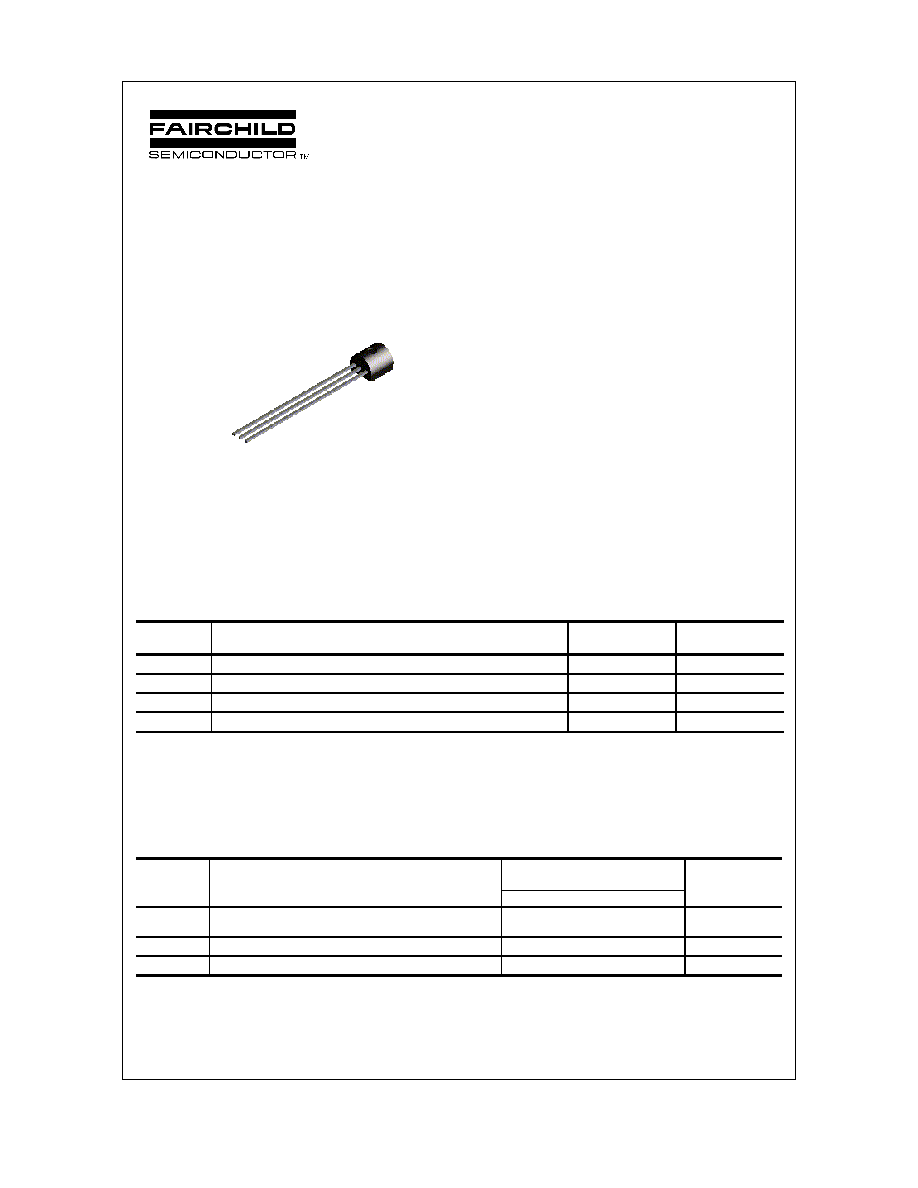
G
S D
TO-92
PN5432/PN5433/PN5434, Rev B
PN5432 / PN5433 / PN5434
Electrical Characteristics
TA = 25°C unless otherwise noted
OFF CHARACTERISTICS
Symbol
Parameter
Test Conditions
Min
Max
Units
ON CHARACTERISTICS
SMALL SIGNAL CHARACTERISTICS
I
DSS
Zero-Gate Voltage Drain Current*
V
DS
= 15 V, V
GS
= 0
5432
5433
5434
150
100
30
mA
mA
mA
V
DS(on)
Drain-Source On Voltage
I
D
= 10 mA, V
GS
= 0
5432
5433
5434
50
70
100
mV
mV
mV
r
DS(
on
)
Drain-Source On Resistance
I
D
= 10
mA, V
GS
= 0
5432
5433
5434
I
D
= 0, V
GS
= 0, f = 1.0 kHz
5432
5433
5434
2.0
2.0
5.0
7.0
10
5.0
7.0
10
V
(BR)GSS
Gate-Source Breakdown Voltage
I
G
= 1.0
µ
A, V
DS
= 0
-25
V
I
GSS
Gate Reverse Current
V
GS
= 15 V, V
DS
= 0
V
GS
= 15 V, V
DS
= 0, T
A
= 150
°
C
-200
-200
pA
nA
I
D(off)
Drain Cutoff Leakage Voltage
V
GS
= 10 V, V
DS
= 5.0 V
V
GS
= 10 V, V
DS
= 5.0 V,
T
A
= 150
°
C
-200
-200
pA
nA
V
GS(off)
Gate-Source Cutoff Voltage
V
DS
= 5.0 V, I
D
= 3.0 nA 5432
5433
5434
-4.0
-3.0
-1.0
-10
-9.0
-4.0
V
V
V
N-Channel Switch
(continued)
C
iss
Input Capacitance
V
DS
= 0 , V
GS
= 10 V, f = 1.0 MHz
30
pF
C
rss
Reverse Transfer Capacitance
V
DS
= 0 , V
GS
= 10 V, f = 1.0 MHz
15
pF
*
Pulse Test: Pulse Width
300
µ
s, Duty Cycle
2.0%
t
d
Delay Time
V
DD
= 1.5 V, V
GS(
on)
= 0,
4.0
ns
t
r
Rise Time
I
D(
on
)
= 10 mA
1.0
ns
t
s
Storage Time
V
GS(
off)
= 12 V,
V
DS(
on)
= 50 mV
5432
V
DS(
on)
= 70 mV
5433
V
DS(
on)
= 100 mV
5434
6.0
6.0
6.0
ns
ns
ns
t
f
Fall Time
V
GS(
off)
= 12 V
30
ns
SWITCHING CHARACTERISTICS
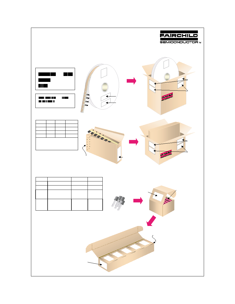
TO-92 Tape and Reel Data
March 2001, Rev. B1
©2001 Fairchild Semiconductor Corporation
TO-92 Packaging
Configuration: Figure 1.0
AMMO PACK OPTION
See Fig 3.0 for 2 Ammo
Pack Options
2000 units per
EO70 box for
std option
FSCINT Label
530mm x 130mm x
83mm
Intermediate box
10,000 units maximum
per
intermediate box
for std option
FSCINT Label
114mm x 102mm x 51mm
Immediate Box
Anti-static
Bubble Sheets
(TO-92) BULK PACKING INFORMATION
EOL
CODE
DESCRIPTION
LEADCLIP
DIMENSION
QUANTITY
J18Z
TO-18 OPTION STD
NO LEAD CLIP
2.0 K / BOX
J05Z
TO-5 OPTION STD
NO LEAD CLIP
1.5 K / BOX
NO EOL
CODE
TO-92 STANDARD
STRAIGHT FOR: PKG 92,
NO LEADCLIP
2.0 K / BOX
BULK OPTION
See Bulk Packing
Information table
375mm x 267mm x 375mm
Intermediate Box
FSCINT
Label
Customized
Label
333mm x 231mm x 183mm
Intermediate Box
FSCINT
Label
Customized
Label
TO-92 TNR/AMMO PACKING INFROMATION
Packing
Style
Quantity
EOL code
Reel
A
2,000
D26Z
E
2,000
D27Z
Ammo
M
2,000
D74Z
P
2,000
D75Z
Unit weight = 0.22 gm
Reel weight with components = 1.04 kg
Ammo weight with components = 1.02 kg
Max quantity per intermediate box = 10,000 units
F63TNR
Label
5 Ammo boxes per
Intermediate Box
Customized
Label
327mm x 158mm x 135mm
Immediate Box
LOT:
CBVK741B019
NSID:
PN2222N
D/C1:
D9842
SPEC REV:
B2
SPEC:
QTY:
10000
QA REV:
FAIRCHILD SEMICONDUCTOR CORPORATION
HTB:B
(FSCINT)
F63TNR
Label
Customized
Label
5 Reels per
Intermediate Box
TAPE and REEL OPTION
See Fig 2.0 for various
Reeling Styles
LOT: CBVK741B019
FSID: PN222N
D/C1: D9842 QTY1:
SPEC REV:
SPEC:
QTY: 2000
D/C2:
QTY2:
CPN:
N/F: F (F63TNR)3
F63TNR Label sample
FSCINT Label sample
C
5 EO70 boxes per
intermediate Box
ustomized
Label
94 (NON PROELECTRON
SERIES), 96
L34Z
TO-92 STANDARD
STRAIGHT FOR: PKG 94
NO LEADCLIP
2.0 K / BOX
(PROELECTRON SERIES
BCXXX, BFXXX, BSRXXX),
97, 98
TO-92 Tape and Reel Data, continued
September 1999, Rev. B
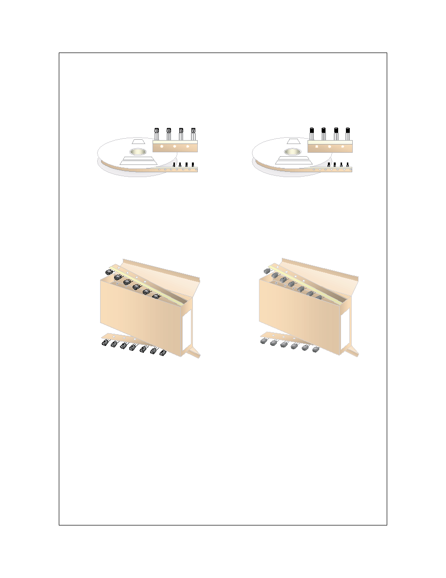
TO-92 Reeling Style
Configuration: Figure 2.0
Style "A", D26Z, D70Z (s/h)
Machine Option "A" (H)
Style "E", D27Z, D71Z (s/h)
Machine Option "E" (J)
FIRST WIRE OFF IS EMITTER
ADHESIVE TAPE IS ON THE TOP SIDE
FLAT OF TRANSISTOR IS ON BOTTOM
ORDER STYLE
D75Z (P)
FIRST WIRE OFF IS COLLECTOR
ADHESIVE TAPE IS ON THE TOP SIDE
FLAT OF TRANSISTOR IS ON TOP
ORDER STYLE
D74Z (M)
TO-92 Radial Ammo Packaging
Configuration: Figure 3.0
FIRST WIRE OFF IS EMITTER (ON PKG. 92)
ADHESIVE TAPE IS ON BOTTOM SIDE
FLAT OF TRANSISTOR IS ON BOTTOM
FIRST WIRE OFF IS COLLECTOR (ON PKG. 92)
ADHESIVE TAPE IS ON BOTTOM SIDE
FLAT OF TRANSISTOR IS ON TOP
ITEM DESCRIPTION
Base of Package to Lead Bend
Component Height
Lead Clinch Height
Component Base Height
Component Alignment ( side/side )
Component Alignment ( front/back )
Component Pitch
Feed Hole Pitch
Hole Center to First Lead
Hole Center to Component Center
Lead Spread
Lead Thickness
Cut Lead Length
Taped Lead Length
Taped Lead Thickness
Carrier Tape Thickness
Carrier Tape Width
Hold - down Tape Width
Hold - down Tape position
Feed Hole Position
Sprocket Hole Diameter
Lead Spring Out
SYMBOL
b
Ha
HO
H1
Pd
Hd
P
PO
P1
P2
F1/F2
d
L
L1
t
t1
W
WO
W1
W2
DO
S
DIMENSION
0.098 (max)
0.928 (+/- 0.025)
0.630 (+/- 0.020)
0.748 (+/- 0.020)
0.040 (max)
0.031 (max)
0.500 (+/- 0.020)
0.500 (+/- 0.008)
0.150 (+0.009, -0.010)
0.247 (+/- 0.007)
0.104 (+/- 0 .010)
0.018 (+0.002, -0.003)
0.429 (max)
0.209 (+0.051, -0.052)
0.032 (+/- 0.006)
0.021 (+/- 0.006)
0.708 (+0.020, -0.019)
0.236 (+/- 0.012)
0.035 (max)
0.360 (+/- 0.025)
0.157 (+0.008, -0.007)
0.004 (max)
Note : All dimensions are in inches.
ITEM DESCRIPTION
SYSMBOL
MINIMUM
MAXIMUM
Reel Diameter
D1
13.975
14.025
Arbor Hole Diameter (Standard)
D2
1.160
1.200
(Small Hole)
D2
0.650
0.700
Core Diameter
D3
3.100
3.300
Hub Recess Inner Diameter
D4
2.700
3.100
Hub Recess Depth
W1
0.370
0.570
Flange to Flange Inner Width
W2
1.630
1.690
Hub to Hub Center Width
W3
2.090
Note: All dimensions are inches
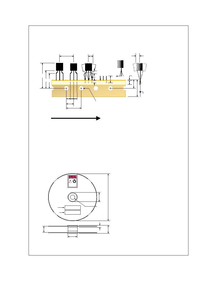
TO-92 Tape and Reel Taping
Dimension Configuration: Figure 4.0
Ha
H1 HO
PO
P2
P1 F1
DO
P
Pd
b
d
L1
L
S
WO
W2
W
t
t1
Hd
W1
TO-92 Reel
Configuration: Figure 5.0
User Direction of Feed
SEN SI TIVE D EVICES
ELECT ROSTATIC
D1
D3
Customized Label
W2
W1
W3
F63TNR Label
D4
D2
TO-92 Tape and Reel Data, continued
July 1999, Rev. A