Äîêóìåíòàöèÿ è îïèñàíèÿ www.docs.chipfind.ru
4/10/03
SMALL OUTLINE OPTOCOUPLERS
TRANSISTOR OUTPUT
Page 1 of 10
© 2003 Fairchild Semiconductor Corporation
MOC205-M
MOC206-M
MOC207-M
MOC208-M
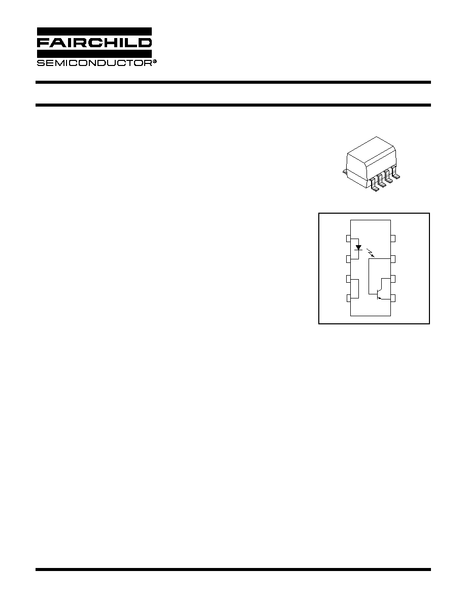
DESCRIPTION
These devices consist of a gallium arsenide infrared emitting diode optically coupled to a
monolithic silicon phototransistor detector, in a surface mountable, small outline, plastic
package. They are ideally suited for high density applications, and eliminate the need for
through - the - board mounting.
FEATURES
· U.L. Recognized (File #E90700, Volume 2)
· VDE Recognized (File #136616) (add option "V" for VDE approval, i.e, MOC205V-M)
· Closely Matched Current Transfer Ratios
· Convenient Plastic SOIC-8 Surface Mountable Package Style
· Minimum BV
CEO
of 70 Volts Guaranteed
· Standard SOIC-8 Footprint, with 0.050" Lead Spacing
· Compatible with Dual Wave, Vapor Phase and IR Reflow Soldering
· High Input-Output Isolation of 2500 V
AC(rms)
Guaranteed
APPLICATIONS
· Feedback Control Circuits
· Interfacing and coupling systems of different potentials and impedances
· General Purpose Switching Circuits
· Monitor and Detection Circuits
BASE
N/C
ANODE
CATHODE
1
2
3
4
5
6
7
8
EMITTER
COLLECTOR
N/C
N/C

4/10/03
Page 2 of 10
© 2003 Fairchild Semiconductor Corporation
SMALL OUTLINE OPTOCOUPLERS
TRANSISTOR OUTPUT
MOC205-M
MOC206-M
MOC207-M
MOC208-M
ABSOLUTE MAXIMUM RATINGS (T
A
= 25°C Unless otherwise specified)
Rating
Symbol
Value
Unit
EMITTER
Forward Current - Continuous
I
F
60
mA
Forward Current - Peak (PW = 100 µs, 120 pps)
I
F
(pk)
1.0
A
Reverse Voltage
V
R
6.0
V
LED Power Dissipation @ T
A
= 25°C
Derate above 25°C
P
D
90
0.8
mW
mW/°C
DETECTOR
V
CEO
70
V
Collector-Emitter Voltage
Emitter-Collector Voltage
V
ECO
7.0
V
Collector-Base Voltage
V
CBO
70
V
Collector Current-Continuous
I
C
150
mA
Detector Power Dissipation @ T
A
= 25°C
Derate above 25°C
P
D
150
1.76
mW
mW/°C
TOTAL DEVICE
Input-Output Isolation Voltage (1,2,3)
(f = 60 Hz, t = 1 min.)
V
ISO
2500
Vac(rms)
Total Device Power Dissipation @ T
A
= 25°C
Derate above 25°C
P
D
250
2.94
mW
mW/°C
Ambient Operating Temperature Range
T
A
-40 to +100
°C
Storage Temperature Range
T
stg
-40 to +150
°C
4/10/03
Page 3 of 10
© 2003 Fairchild Semiconductor Corporation
SMALL OUTLINE OPTOCOUPLERS
TRANSISTOR OUTPUT
MOC205-M
MOC206-M
MOC207-M
MOC208-M
** Typical values at T
A
= 25°C
1. Isolation Surge Voltage, V
ISO
, is an internal device dielectric breakdown rating.
2. For this test, Pins 1 and 2 are common and Pins 5, 6 and 7 are common.
3. V
ISO
rating of 2500 V
AC(rms)
for t = 1 min. is equivalent to a rating of 3,000 V
AC(rms)
for t = 1 sec.
4. Current Transfer Ratio (CTR) = I
C
/I
F
x 100%.
ELECTRICAL CHARACTERISTICS (T
A
= 25°C unless otherwise specified)
Parameter
Test Conditions
Symbol
Min
Typ**
Max
Unit
EMITTER
Input Forward Voltage
(I
F
= 10 mA)
V
F
--
1.15
1.5
V
Reverse Leakage Current
(V
R
= 6.0 V)
I
R
--
0.001
100
µA
Input Capacitance
C
IN
--
18
--
pF
DETECTOR
Collector-Emitter Dark Current
(V
CE
= 10 V, T
A
= 25°C)
(V
CE
= 10 V, T
A
= 100°C)
I
CEO1
I
CEO2
--
--
1.0
1.0
50
--
nA
µA
Collector-Emitter Breakdown Voltage
(I
C
= 100 µA)
BV
CEO
70
100
--
V
Emitter-Collector Breakdown Voltage
(I
E
= 100 µA)
BV
ECO
7.0
10
--
V
Collector-Emitter Capacitance
(f = 1.0 MHz, V
CE
= 0)
C
CE
--
7.0
--
pF
COUPLED
Collector-Output Current
(4)
MOC205-M
MOC206-M
MOC207-M
MOC208-M
(I
F
= 10 mA, V
CE
= 10 V)
CTR
40
63
100
40
--
--
--
--
80
125
200
125
%
Isolation Surge Voltage
(1,2,3)
(f = 60 Hz AC Peak, t = 1 min.)
V
ISO
2500
--
--
Vac(rms)
Isolation Resistance
(2)
(V = 500 V)
R
ISO
10
11
--
--
Collector-Emitter Saturation Voltage
(I
C
= 2 mA, I
F
= 10 mA)
V
CE (sat)
--
--
0.4
V
Isolation Capacitance
(2)
(V = 0 V, f = 1 MHz)
C
ISO
--
0.2
--
pF
Turn-On Time
(I
C
= 2.0 mA, V
CC
= 10 V,
R
L
= 100
) (Fig. 6)
t
on
--
7.5
--
µs
Turn-Off Time
(I
C
= 2.0 mA, V
CC
= 10 V,
R
L
= 100
) (Fig. 6)
t
off
--
5.7
--
µs
Rise Time
(I
C
= 2.0 mA, V
CC
= 10 V,
R
L
= 100
) (Fig. 6)
t
r
--
3.2
--
µs
Fall Time
(I
C
= 2.0 mA, V
CC
= 10 V,
R
L
= 100
) (Fig. 6)
t
f
--
4.7
--
µs
4/10/03
Page 4 of 10
© 2003 Fairchild Semiconductor Corporation
SMALL OUTLINE OPTOCOUPLERS
TRANSISTOR OUTPUT
MOC205-M
MOC206-M
MOC207-M
MOC208-M
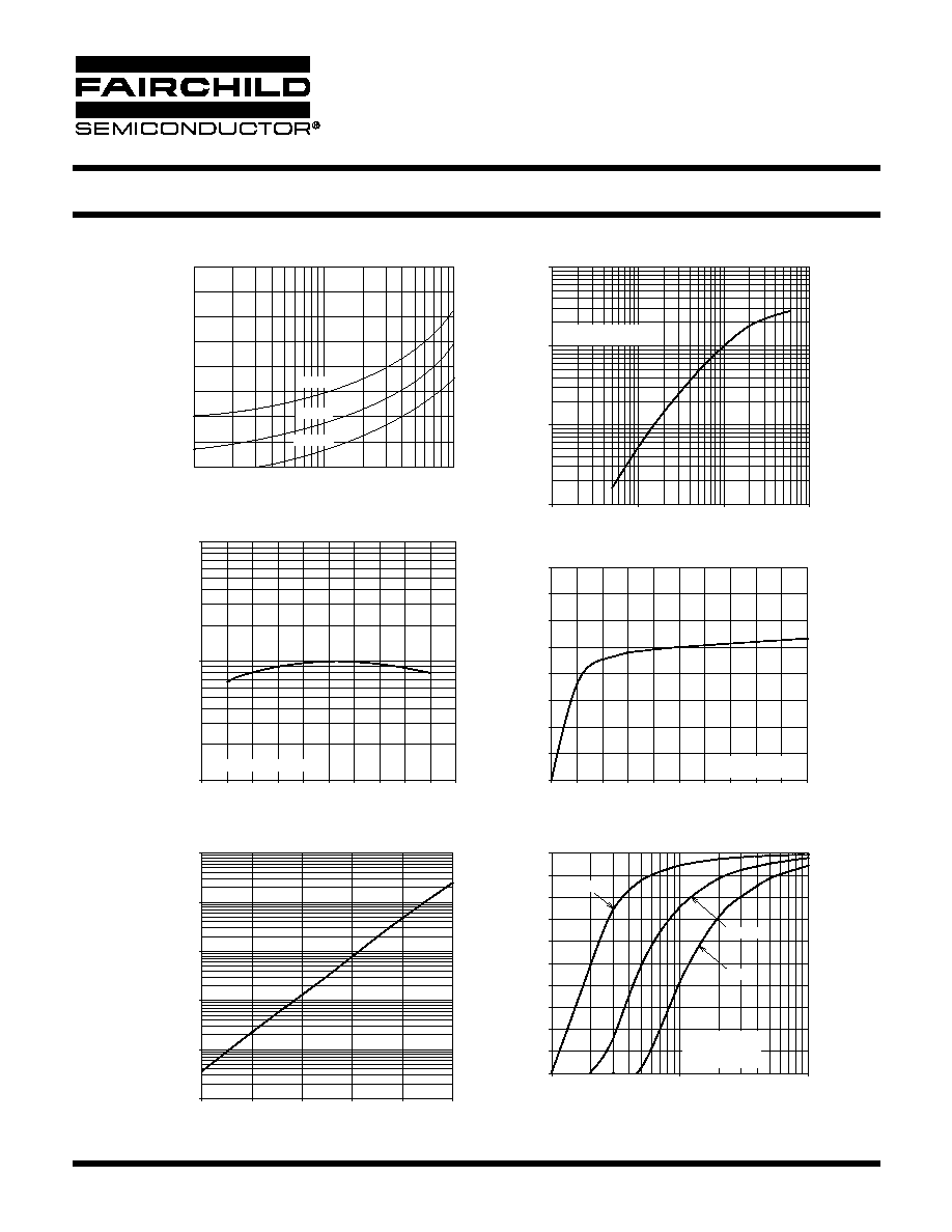
Fig. 2 Output Curent vs. Input Current
I
F
- LED INPUT CURRENT (mA)
0.1
1
10
100
I
C
- OU
T
P
U
T
C
O
L
L
EC
T
O
R
C
U
RR
EN
T
(
N
O
R
M
A
LI
Z
E
D
)
0.01
0.1
1
10
V
CE
= 5V
NORMALIZED TO I
F
= 10mA
Fig. 3 Output Current vs. Ambient Temperature
T
A
- AMBIENT TEMPERATURE (
°C)
-80
-60
-40
-20
0
20
40
60
80
100
120
I
C
- OU
T
P
U
T
C
O
L
L
EC
T
O
R
CU
R
R
E
N
T (
N
O
R
M
A
L
I
ZE
D
)
0.1
1
10
NORMALIZED TO T
A
= 25
°C
Fig. 4 Output Current vs. Collector - Emitter Voltage
V
CE
- COLLECTOR -EMITTER VOLTAGE (V)
0
1
2
3
4
5
6
7
8
9
10
I
C
- O
U
T
P
U
T
C
O
L
L
EC
TO
R
CU
R
R
E
N
T
(
N
OR
M
A
L
I
Z
E
D
)
0.0
0.2
0.4
0.6
0.8
1.0
1.2
1.4
1.6
I
F
= 10mA
NORMALIZED TO V
CE
= 5V
Fig. 5 Dark Current vs. Ambient Temperature
Fig. 6 CTR vs. R
BE
(Unsaturated)
T
A
- AMBIENT TEMPERATURE (
°C)
0
20
40
60
80
100
I
CE
O
- C
O
L
L
E
C
T
O
R -
E
M
I
T
T
E
R
D
A
RK
CU
RR
E
N
T
(
n
A
)
0.1
1
10
100
1000
10000
V
CE
=10V
I
F
- LED FORWARD CURRENT (mA)
V
F
- FOR
W
ARD
V
O
L
T
A
G
E (V)
Fig. 1 LED Forward Voltage vs. Forward Current
1
10
100
1.0
1.1
1.2
1.3
1.4
1.5
1.6
1.7
1.8
T
A
= 55
°C
T
A
= 25
°C
T
A
= 100
°C
R
BE
- BASE RESISTANCE (k
)
10
100
100 0
NORMALIZED CTR
0.0
0.1
0.2
0.3
0.4
0.5
0.6
0.7
0.8
0.9
1.0
I
F
mA
I
F
=
I
F
= 20
10mA
= 5mA
V
CE
= 5V, T
A
= 25°C
Normalized to:
CTR at R
BE
= Open
4/10/03
Page 5 of 10
© 2003 Fairchild Semiconductor Corporation
SMALL OUTLINE OPTOCOUPLERS
TRANSISTOR OUTPUT
MOC205-M
MOC206-M
MOC207-M
MOC208-M
NORM
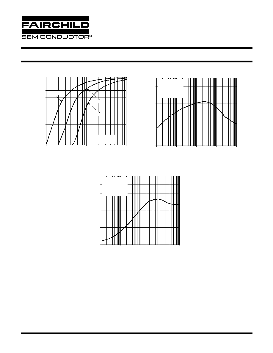
Fig. 8 Normalized t
on
vs. R
BE
Fig. 9 Normalized t
off
vs. R
BE
Fig. 7 CTR vs. R
BE
(Saturated)
R
BE
- BASE RESISTANCE (k
)
10
100
1000
NORM
AL
IZE
D CT
R
0.0
0.1
0.2
0.3
0.4
0.5
0.6
0.7
0.8
0.9
1.0
I
F
= 20mA
I
F
= 10mA
I
F
= 5mA
V
CE
= 0.3V, T
A
= 25
°C
Normalized to:
CTR at R
BE
= Open
R
BE
- BASE RESISTANCE (M
)
(M
)
0.01
0.1
1
10
100
ALIZED t
on
0.0
0.5
1.0
1.5
2.0
2.5
3.0
3.5
4.0
V
CC
= 10V
I
C
= 2mA
R
L
= 100
NORMALIZED TO :
t
on
AT R
BE
= OPEN
R
BE
- BASE RESISTANCE
0.01
0.1
1
10
100
NORM
ALIZED t
of
ff
0.0
0.2
0.4
0.6
0.8
1.0
1.2
1.4
1.6
V
CC
= 10V
I
C
= 2mA
R
L
= 100
NORMALIZED TO :
t
offf
AT R
BE
= OPEN
4/10/03
Page 6 of 10
© 2003 Fairchild Semiconductor Corporation
SMALL OUTLINE OPTOCOUPLERS
TRANSISTOR OUTPUT
MOC205-M
MOC206-M
MOC207-M
MOC208-M
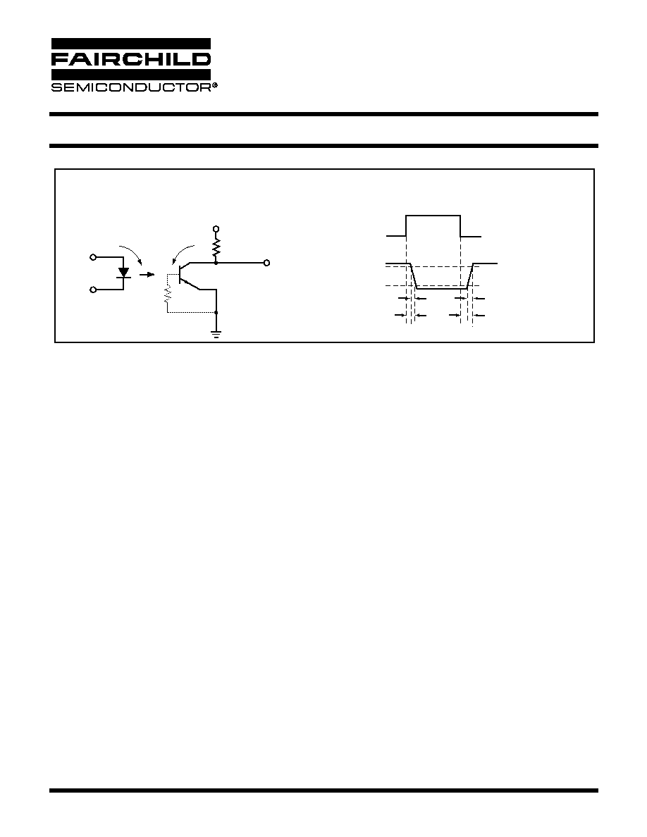
OUTPUT PULSE
INPUT PULSE
TEST CIRCUIT
WAVE FORMS
t
r
t
f
INPUT
I
F
R
L
R
BE
V
CC
= 10V
OUTPUT
t
on
10%
90%
t
off
Figure 6. Switching Time Test Circuit and Waveforms
I
C
Adjust I
F
to produce I
C
= 2 mA
4/10/03
Page 7 of 10
© 2003 Fairchild Semiconductor Corporation
SMALL OUTLINE OPTOCOUPLERS
TRANSISTOR OUTPUT
MOC205-M
MOC206-M
MOC207-M
MOC208-M
Package Dimensions (Surface Mount)
8-Pin Small Outline
Lead Coplanarity : 0.004 (0.10) MAX
PIN 1
ID.
0.202 (5.13)
0.182 (4.63)
0.021 (0.53)
0.011 (0.28)
0.050 (1.27)
TYP
0.164 (4.16)
0.144 (3.66)
0.244 (6.19)
0.224 (5.69)
0.143 (3.63)
0.123 (3.13)
0.008 (0.20)
0.003 (0.08)
0.010 (0.25)
0.006 (0.16)
SEATING PLANE
0.024 (0.61)
0.050 (1.27)
0.155 (3.94)
0.275 (6.99)
0.060 (1.52)
4/10/03
Page 8 of 10
© 2003 Fairchild Semiconductor Corporation
SMALL OUTLINE OPTOCOUPLERS
TRANSISTOR OUTPUT
MOC205-M
MOC206-M
MOC207-M
MOC208-M
ORDERING INFORMATION
MARKING INFORMATION
Option
Order Entry Identifier
Description
V
V
VDE 0884
R1
R1
Tape and reel (500 units per reel)
R1V
R1V
VDE 0884, Tape and reel (500 units per reel)
R2
R2
Tape and reel (2500 units per reel)
R2V
R2V
VDE 0884, Tape and reel (2500 units per reel)
1
2
6
4
3
5
Definitions
1
Fairchild logo
2
Device number
3
VDE mark (Note: Only appears on parts ordered with VDE
option See order entry table)
4
One digit year code, e.g., `3'
5
Two digit work week ranging from `01' to `53'
6
Assembly package code
205
S
YY
X
V
4/10/03
Page 9 of 10
© 2003 Fairchild Semiconductor Corporation
SMALL OUTLINE OPTOCOUPLERS
TRANSISTOR OUTPUT
MOC205-M
MOC206-M
MOC207-M
MOC208-M
Carrier Tape Specifications
Reflow Profile
4.0
± 0.10
Ø1.5 MIN
User Direction of Feed
2.0
± 0.05
1.75
± 0.10
5.5
± 0.05
12.0
± 0.3
8.0
± 0.10
0.30 MAX
8.3
± 0.10
3.50
± 0.20
0.1 MAX
6.40
± 0.20
5.20
± 0.20
Ø1.5
± 0.1/-0
Ramp up = 210
°C/sec
· Peak reflow temperature: 245
°C (package surface temperature)
· Time of temperature higher than 183
°C for 120180 seconds
· One time soldering reflow is recommended
230
°C, 1030 s
Time (Minute)
0
300
250
200
150
100
50
0
0.5
1
1.5
2
2.5
3
3.5
4
4.5
T
emperature (
°
C)
Time above 183
°C, 120180 sec
245
°C peak

4/10/03
LIFE SUPPORT POLICY
FAIRCHILD'S PRODUCTS ARE NOT AUTHORIZED FOR USE AS CRITICAL COMPONENTS IN LIFE SUPPORT DEVICES
OR SYSTEMS WITHOUT THE EXPRESS WRITTEN APPROVAL OF THE PRESIDENT OF FAIRCHILD SEMICONDUCTOR
CORPORATION. As used herein:
1. Life support devices or systems are devices or systems
which, (a) are intended for surgical implant into the body, or
(b) support or sustain life, and (c) whose failure to perform
when properly used in accordance with instructions for use
provided in the labeling, can be reasonably expected to
result in a significant injury of the user.
2. A critical component in any component of a life support
device or system whose failure to perform can be
reasonably expected to cause the failure of the life support
device or system, or to affect its safety or effectiveness.
DISCLAIMER
FAIRCHILD SEMICONDUCTOR RESERVES THE RIGHT TO MAKE CHANGES WITHOUT FURTHER NOTICE TO
ANY PRODUCTS HEREIN TO IMPROVE RELIABILITY, FUNCTION OR DESIGN. FAIRCHILD DOES NOT ASSUME
ANY LIABILITY ARISING OUT OF THE APPLICATION OR USE OF ANY PRODUCT OR CIRCUIT DESCRIBED HEREIN;
NEITHER DOES IT CONVEY ANY LICENSE UNDER ITS PATENT RIGHTS, NOR THE RIGHTS OF OTHERS.
Page 10 of 10
© 2003 Fairchild Semiconductor Corporation
SMALL OUTLINE OPTOCOUPLERS
TRANSISTOR OUTPUT
MOC205-M
MOC206-M
MOC207-M
MOC208-M