© 2000 Fairchild Semiconductor Corporation
DS005343
www.fairchildsemi.com
January 1988
Revised August 2000
MM74HC597 8-Bi
t Shif
t Regi
ster
s
wi
th Input
L
a
tches
MM74HC597
8-Bit Shift Registers with Input Latches
General Description
This high speed register utilizes advanced silicon-gate
CMOS technology. It has the high noise immunity and low
power consumption of standard CMOS integrated circuits,
as well as the ability to drive 10 LS-TTL loads.
The MM74HC597 comes in a 16-pin package and consists
of an 8-bit storage latch feeding a parallel-in, serial-out
8-bit shift register. Both the storage register and shift regis-
ter have positive-edge triggered clocks. the shift register
also has direct load (from storage) and clear inputs.
The 74HC logic family is speed, function, and pin-out com-
patible with the standard 74LS logic family. All inputs are
protected from damage due to static discharge by internal
diode clamps to V
CC
and ground.
Features
s
8-bit parallel storage register inputs
s
Wide operating voltage range: 2V6V
s
Shift register has direct overriding load and clear
s
Guaranteed shift frequency: DC to 30 MHz
s
Low quiescent current: 80
µ
A maximum
Ordering Code:
Devices also available in Tape and Reel. Specify by appending the suffix letter "X" to the ordering code.
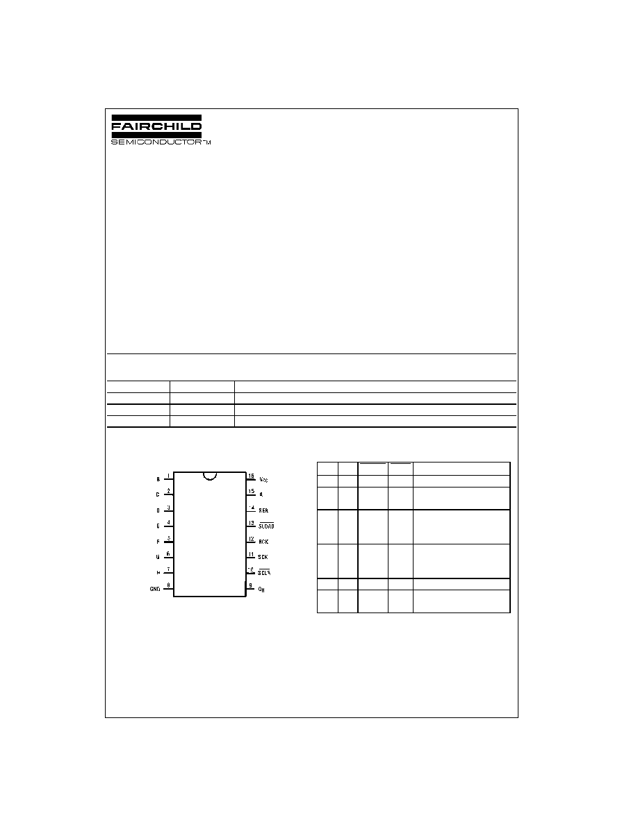
Connection Diagram
Top View
Truth Table
Order Number
Package Number
Package Description
MM74HC597M
M16A
16-Lead Small Outline Integrated Circuit (SOIC), JEDEC MS-012, 0.150 Narrow
MM74HC597SJ
M16D
16-Lead Small Outline Package (SOP), EIAJ TYPE II, 5.3mm Wide
MM74HC597N
N16E
16-Lead Plastic Dual-In-Line Package (PDIP), JEDEC MS-001, 0.300 Wide
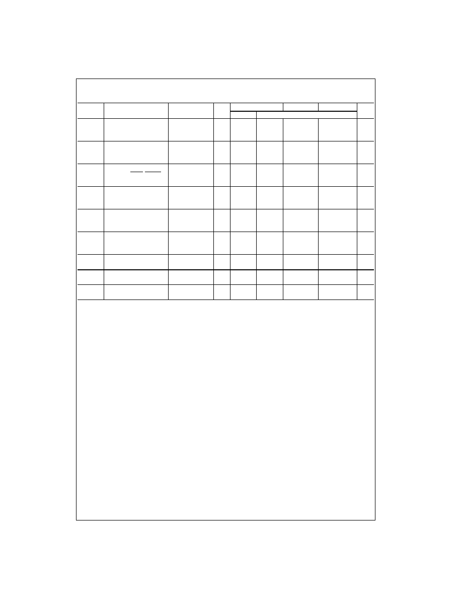
RCK SCK SLOAD SCLR
Function
X
X
X
Data Loaded to input latches
X
L
H
Data loaded from inputs to
shift register
No
Data transferred from
clock
X
L
H
input latches to shift
edge
register
X
X
L
L
Invalid logic, state of
shift register indeterminate
when signals removed
X
X
H
L
Shift register cleared
X
H
H
Shift register clocked
Q
n
=
Q
n
-
1, Q
0
=
SER
www.fairchildsemi.com
2
MM
74HC597
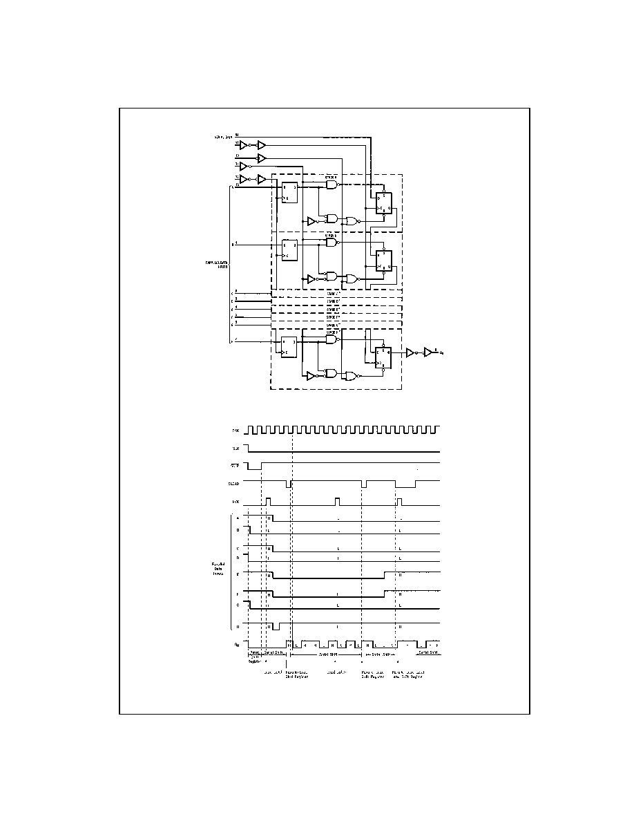
Functional Block Diagram
(Positive Logic)
Timing Diagram
3
www.fairchildsemi.com
MM74HC597
Absolute Maximum Ratings
(Note 1)
(Note 2)
Recommended Operating
Conditions
Note 1: Absolute Maximum Ratings are those values beyond which dam-
age to the device may occur.
Note 2: Unless otherwise specified all voltages are referenced to ground.
Note 3: Power Dissipation temperature derating -- plastic "N" package:
-
12 mW/
°
C from 65
°
C to 85
°
C.
DC Electrical Characteristics
(Note 4)
Note 4: For a power supply of 5V
±
10% the worst case output voltages (V
OH
, and V
OL
) occur for HC at 4.5V. Thus the 4.5V values should be used when
designing with this supply. Worst case V
IH
and V
IL
occur at V
CC
=
5.5V and 4.5V respectively. (The V
IH
value at 5.5V is 3.85V.) The worst case leakage cur-
rent (I
IN
, I
CC
, and I
OZ
) occur for CMOS at the higher voltage and so the 6.0V values should be used.
Note 5: V
IL
limits are currently tested at 20% of V
CC
. The above V
IL
specification (30% of V
CC
) will be implemented no later than Q1, CY'89.
Supply Voltage (V
CC
)
-
0.5 to
+
7.0V
DC Input Voltage (V
IN
)
-
1.5 to V
CC
+
1.5V
DC Output Voltage (V
OUT
)
-
0.5 to V
CC
+
0.5V
Clamp Diode Current (I
IK
, I
OK
)
±
20 mA
DC Output Current, per pin (I
OUT
)
±
25 mA
DC V
CC
or GND Current, per pin (I
CC
)
±
70 mA
Storage Temperature Range (T
STG
)
-
65
°
C to
+
150
°
C
Power Dissipation (P
D
)
(Note 3)
600 mW
S.O. Package only
500 mW
Lead Temperature (T
L
)
(Soldering 10 seconds)
260
°
C
Min
Max
Units
Supply Voltage (V
CC
)
2
6
V
DC Input or Output Voltage
(V
IN
, V
OUT
)
0
V
CC
V
Operating Temperature Range (T
A
)
-
40
+
85
°
C
Input Rise or Fall Times
(t
r
, t
f
) V
CC
=
2.0V
1000
ns
V
CC
=
4.5V
500
ns
V
CC
=
6.0V
400
ns
Symbol
Parameter
Conditions
V
CC
T
A
=
25
°
C
T
A
=
-
40 to 85
°
C T
A
=
-
55 to 125
°
C
Units
Typ
Guaranteed Limits
V
IH
Minimum HIGH Level
2.0V
1.5
1.5
1.5
V
Input Voltage
4.5V
3.15
3.15
3.15
6.0V
4.2
4.2
4.2
V
IL
Maximum LOW Level
2.0V
0.5
0.5
0.5
V
Input Voltage
4.5V
1.35
1.35
1.35
(Note 5)
6.0V
1.8
1.8
1.8
V
OH
Minimum HIGH Level
V
IN
=
V
IH
or V
IL
V
Output Voltage
|I
OUT
|
20
µ
A
2.0V
2.0
1.9
1.9
1.9
4.5V
4.5
4.4
4.4
4.4
6.0V
6.0
5.9
5.9
5.9
V
IN
=
V
IH
or V
IL
V
|I
OUT
|
4.0 mA
4.5V
4.2
3.98
3.84
3.7
|I
OUT
|
5.2 mA
6.0V
5.2
5.48
5.34
5.2
V
OL
Maximum LOW Level
V
IN
=
V
IH
or V
IL
V
Output Voltage
|I
OUT
|
20
µ
A
2.0V
0
0.1
0.1
0.1
4.5V
0
0.1
0.1
0.1
6.0V
0
0.1
0.1
0.1
V
IN
=
V
IH
or V
IL
V
|I
OUT
|
4 mA
4.5V
0.2
0.26
0.33
0.4
|I
OUT
|
5.2 mA
6.0V
0.2
0.26
0.33
0.4
I
IN
Maximum Input Current
V
IN
=
V
CC
or GND
6.0V
±
0.1
±
1.0
±
1.0
µ
A
I
CC
Maximum Quiescent
V
IN
=
V
CC
or GND
6.0V
8.0
80
160
µ
A
Supply Current
I
OUT
=
0
µ
A
www.fairchildsemi.com
4
MM
74HC597
AC Electrical Characteristics
V
CC
=
5V, T
A
=
25
°
C, C
L
=
15 pF, t
r
=
t
f
=
6 ns
AC Electrical Characteristics
V
CC
=
2.06.0V, C
L
=
50 pF, t
r
=
t
f
=
6 ns (unless otherwise specified)
Symbol
Parameter
Conditions
Typ
Guaranteed
Units
Limit
f
MAX
Maximum Operating
50
30
MHz
Frequency of SCK
t
PHL
Maximum Propagation
20
30
ns
t
PLH
Delay from SCK to Q
H
t
PHL
Maximum Propagation
20
30
ns
t
PLH
Delay from SLOAD to Q
H
t
PHL
Maximum propagation
SLOAD
=
logic "0"
25
45
ns
t
PLH
Delay from RCK to Q
H
t
PHL
Maximum Propagation
20
30
ns
Delay from SCLR to Q
H
t
REM
Minimum Removal Time,
10
20
ns
SCLR to SCK
t
S
Minimum Setup Time
30
40
ns
from RCK to SCK
t
S
Minimum Setup Time
10
20
ns
from SER to SCK
t
S
Minimum Setup Time
10
20
ns
from inputs A thru H
to RCK
t
H
Minimum Hold Time
-
2
0
ns
t
W
Minimum Pulse Width
10
16
ns
SCK, RCK, SCLR SLOAD
Symbol
Parameter
Conditions
V
CC
T
A
=
25
°
C
T
A
=-
40 to 85
°
C T
A
=-
55 to 125
°
C
Units
Typ
Guaranteed Limits
f
MAX
Maximum Operating
2.0V
10
6.0
4.8
4.0
MHz
Frequency
4.5V
45
30
24
20
6.0V
50
35
28
24
t
PHL
Maximum Propagation
2.0V
62
175
220
263
ns
t
PLH
Delay from SCK to Q
H
4.5V
20
35
44
53
6.0V
18
30
38
45
t
PHL
Maximum Propagation
2.0V
65
175
220
263
ns
t
PLH
Delay from SLOAD to Q
H
4.5V
20
35
44
53
6.0V
18
30
38
45
t
PHL
Maximum Propagation
2.0V
120
205
255
310
ns
t
PLH
Delay from RCK to Q
H
SLOAD
=
Logic "0"
4.5V
30
41
51
62
6.0V
28
35
43
53
t
PHL
Maximum Propagatin
2.0V
66
175
220
263
ns
Delay from SCLR to Q
H
4.5V
20
35
44
53
6.0V
18
30
38
45
t
REM
Minimum Removal Time
2.0V
100
125
150
ns
SCLR to SCK
4.5V
20
25
30
6.0V
17
21
25
t
S
Minimum Setup Time
2.0V
200
250
300
ns
from RCK to SCK
4.5V
40
50
60
6.0V
34
42
50
t
S
Minimum Setup Time
2.0V
100
125
150
ns
from SER to SCK
4.5V
20
25
30
6.0V
17
21
25
5
www.fairchildsemi.com
MM74HC597
AC Electrical Characteristics
(Continued)
Note 6: C
PD
determines the no load dynamic power consumption, P
D
=
C
PD
V
CC
2
f
+
I
CC
V
CC
, and the no load dynamic current consumption,
I
S
=
C
PD
V
CC
f
+
I
CC
.
Symbol
Parameter
Conditions
V
CC
T
A
=
25
°
C
T
A
=-
40 to 85
°
C T
A
=-
55 to 125
°
C
Units
Typ
Guaranteed Limits
t
S
Minimum Setup Time
2.0V
100
125
150
ns
from Inputs A thru H
4.5V
20
25
30
to RCK
6.0V
17
21
25
t
H
Minimum Hold Time
2.0V
0
0
0
ns
4.5V
0
0
0
6.0V
0
0
0
t
W
Minimum Pulse Width
2.0V
30
80
100
120
ns
SCK, RCK, SCLR, SLOAD
4.5V
9
16
20
24
6.0V
8
14
18
20
t
r
, t
f
Maximum Input Rise and
2.0V
1000
1000
1000
ns
Fall Time
4.5V
500
500
500
6.0V
400
400
400
t
THL
, t
TLH
Maximum Output
2.0V
30
75
95
110
ns
Rise and Fall Time
4.5V
10
15
19
22
6.0V
8
13
16
19
t
THL
, t
TLH
Maximum Output
2.0V
75
95
110
ns
Rise and Fall Time
4.5V
15
19
22
ns
6.0V
13
16
19
ns
C
PD
Power Dissipation
87
pF
Capacitance, Outputs (Note 6)
C
IN
Maximum Input
5
10
10
10
pF
Capacitance
C
OUT
Maximum Output
15
20
20
20
pF
Capacitance