©2001 Fairchild Semiconductor Corporation
www.fairchildsemi.com
Rev. 1.0.0
Features
· Low Quiescent Current
· Low Dropout Voltage
· Low Temperature Coefficient
· Tight Line and Load Regulation
· Guaranteed 100mA Output Current
· Internal Short Current & Thermal Limit
· Error Signals of Output Dropout (8 pin Versions Only)
· External Shut-down ( 8 pin Versions Only)
Description
The LP2951 is an adjustable micro power voltage regulator
suitable for use in battery-powered systems. This regulator
has various functions such as alarm which warns of a low
output voltage, often due to falling batteries on the input, the
external shutdown which enables the regulator to be
switched on and off, current and temperature limiting.
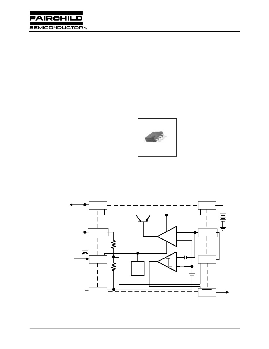
Internal Block Diagram
OUT(1)
PROGRAM
(2)
SHUTDOWN(3)
GROUND(4)
ERROR(5)
TAP(6)
FEEDBACK(7)
INPUT(8)
C1
+
+
+
+
FROM
EXTERNAL
INPUT
+
+
+
+
1.25V
REFERENCE
-
-
-
-
+
+
+
+
+
+
+
+
OFFSE
T
-
-
-
-
+
+
+
+
ERROR
AMPLIFIER
ERROR
COMPARATO
R
TO
EXTERNAL
INPUT
SCP
COMPARATOR
LP2951
Adjustable Micro Power Voltage Regulator
8-SOP
1
LP2951
2
Absolute Maximum Ratings
Parameter
Symbol
Value
Unit
Input Supply Voltage
V
IN
-0.3 ~ +30
V
Power Dissipation
P
D
Internally Limited
W
Thermal Resistance Junction-Air
R
JA
127.5
°
C/W
Storage Temperature Range
T
STG
-65 ~ +150
°
C
Operating Junction Temperature Range
T
OPR
-40 ~ +125
°
C

LP2951
3
Electrical Characteristics
(Refer to the test circuit, Ta = 25
°
C, unless otherwise specified, )
Note :
1. Output or reference voltage temperature coefficient is defined as the worst case voltage change divided by the total
temperature range.
2. Regulation is measured at constant junction temperature , using pulse testing with a low duty cycle.
3. V
ref
V
out
(V
in
- 1V), 2.5V
V
in
28V, 100uA
I
L
100mA, T
A
T
AMAX
.
4. Threshold and hysteresis are expressed in terms of voltage differential at the Feedback terminal below the normal
reference . To express these thresholds in terms of output voltage change , multiply by the error amplifier gain
= VO / VREF = (R1 + R2) / R2 .
5. Vshutdown
0.6 V , V
OUT
=ON , Vshutdown
2.0 V, V
OUT
= OFF.
Parameter
Symbol
Conditions
Min. Typ. Max.
Unit
ALL VOLTAGE OPTIONS
Output Voltage Temperature Coefficient
V
/
T
(Note1)
-
50
-
ppm/
°
C
Line Regulation (Note2)
V
(Vo + 1)V
V
IN
28V
I
L
= 50mA
-
-
0.4
%
Load Regulation (Note2)
V
100uA
I
L
100mA
-
-
0.3
%
Dropout Voltage
V
D
I
L
= 100uA
-
-
150
mV
I
L
= 100mA
-
-
600
mV
Ground Current
I
G
I
L
= 100uA
-
-
140
uA
I
L
= 100mA
-
-
7
mA
Current Limit
I
CL
V
O
= 0V
110
165
220
mA
8-PIN VERSIONS ONLY
Reference Voltage
V
REF
(Note3)
1.235 1.26 1.285
V
V
REF
1.225 1.26 1.295
V
ERROR COMPARATOR
Output Low Voltage
V
OL
V
IN
= (Vo - 0.5)V, I
OL
=400uA
-
150
400
mV
High Threshold Voltage
V
TH
(Note4)
25
60
-
mV
Low Threshold Voltage
V
TL
(Note4)
-
75
140
mV
Hysteresis
V
HYS
(Note4)
-
15
-
mV
SHUTDOWN INPUT
Shutdown Threshold Range
V
SD
(Note5)
0.6
1.3
2.0
V
Shutdown Input Current
I
SD
V
SD
= 2.4V
-
30
100
uA
V
SD
= 28V
-
450
750
uA
LP2951
4
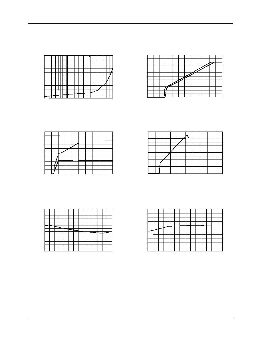
Typical Performance Characteristics
Figure 1. Quiescent Current
Figure 2. Dropout Characteristics
Figure 3. Input Current
Figure 4. Input Current
Figure 6. Short Circuit Current
Figure 5. Output Voltage vs. Temperature
0.1 1 10 100
0.4
0.8
1.2
1.6
2.0
G
R
O
U
N
D
CU
RRE
N
T
(
m
A)
LOAD CURRENT(mA)
0 2 4 6 8 10
0
50
100
150
200
250
I
N
P
U
T
CU
RRE
N
T
(
u
A)
INPUT VOLTAGE(V)
-50 -25 0 25 50 75 100 125
4.94
4.96
4.98
5.00
5.02
5.04
5.06
O
U
TP
U
T
V
O
LTA
G
E
(
V
)
TEMPERATURE(
o
C)
0 1 2 3 4 5 6
0
1
2
3
4
5
6
O
U
TP
U
T
V
O
LTA
G
E
(
V
INPUT VO L T AG E(V)
0 2 4 6 8 10
0
20
40
60
80
100
120
I
N
P
U
T C
U
R
R
E
N
T(
mA
)
I
NPUT VOLT AGE(V
)
-50 -25 0 25 50 75 10 0 12 5
10 0
12 0
14 0
16 0
18 0
20 0
SH
OR
T CI
R
C
U
I
T
C
U
RREN
T
(
m
A
TEMP ERATURE(
o
C)
5V OUTPUT
R
L
=50K
R
L
=50
5V OUTPUT
R
L
=50K
R
L
=
R
L
=50
5V OUTPUT
LP2951
5
Typical Performance Characteristics (Continued)
T
YPICAL PERFORMANCE CHARACTERISTICS (Continued )
-50
-25
0
25
50
75
100
125
0
100
200
300
400
500
600
D
R
O
P
O
U
T V
O
LTA
G
E
(
V
)
TEMPERATURE(
o
C)
Fig. 7 Dropout
Voltage
0.1
1
10
100
0
100
200
300
400
500
D
R
O
P
O
U
T
VO
L
T
AG
E
(
m
V
)
OUTPUT CURRENT(mA
)
Fig. 8 Dropout
Voltage
I
L
= 100mA
I
L
= 100
µ
µ
µ
µ
A
T
J
= 25
o
C
Figure 7. Dropout Voltage
Figure 8. Dropout Voltage