©2001 Fairchild Semiconductor Corporation
www.fairchildsemi.com
Rev.1.0.2
Features
· Wide Operating Frequency Range Up to 150Khz
· Lowest Cost SMPS Solution
· Lowest External Components
· Low Start-up Current (max:170uA)
· Low Operating Current (max:12mA)
· Internal High Voltage SenseFET
· Over Voltage Protection With Latch Mode (Min23V)
· Over Load Protection With Latch Mode
· Over Current Protection With Latch Mode
· Internal Thermal Protection With Latch Mode
· Pulse By Pulse Over Current Limiting
· Under Voltage Lockout With Hysteresis
· External Sync. Terminal
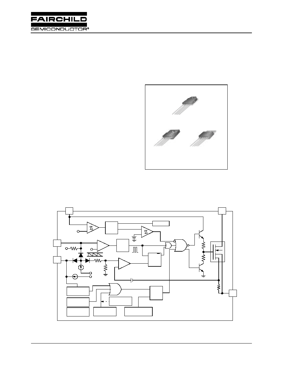
TO-3P-5L
1. Drain 2. Gnd 3. V
CC
4. FeedBack 5. Sync.
TO-220F-5L
1
1
TO-220-5L
1
Internal Block Diagram
+
-
-
+
+
-
+
-
V
CC
Soft Start
& Sync
3
4
5
Vref
V
CC
UVLO
15/9V
Feedback
VREF
Vth.sy
7V
6V
4
µ
A
OSC
VREF
V
CC
2.5V
R
0.95mA
OLP
(Vfb=7.5V)
TSD
(Tj=160
°
C)
OVP
(V
CC
=25V)
OCP
(V
S
=1.1V)
1
µ
s Window
Open Circuit
Power-on Reset
(VCC=6.5V)
S
R
Q
Shutdown Latch
Voffset
S
R
Q
CLK
2.5V
Bias
VREF UVLO
1
2
Drain
GND
V
S
SenseFET
Rsense
KA5S-SERIES
KA5S0765C/KA5S09654QT/KA5S0965/
KA5S12656/KA5S1265
Fairchild Power Switch(FPS)

KA5S-SERIES KA5S0765C/KA5S09654QT/KA5S0965/KA5S12656/KA5S1265
2
Absolute Maximum Ratings
(Ta=2
5
°
C, unless otherwise specified)
Characteristic
Symbol
Value
Unit
KA5S0765C
Maximum drain voltage
V
D,MAX
650
V
Drain-gate voltage(R
GS
=1M
)
V
DGR
650
V
Gate-source(GND) voltage
V
GS
±30
V
Drain current pulsed
(1)
I
DM
28
ADC
Continuous drain current (Tc = 25
°
C)
I
D
7.0
ADC
Continuous drain current (Tc = 100
°
C)
I
D
5.6
ADC
Single pulsed avalanch current
(3)
(Energy
(2)
)
I
AS
(E
AS
)
20(570)
A(mJ)
Maximum supply voltage
V
CC,MAX
30
V
Input voltage range
V
FB
-0.3 to V
CC
V
V
SS
-0.3 to 8
V
Total power dissipation
P
D
(Watt H/S)
135
W
Derating
1.1
W /
°
C
Operating junction temperature.
T
J
+160
°
C
Operating ambient temperature.
T
A
-25 to +85
°
C
Storage temperature range.
T
STG
-55 to +150
°
C
KA5S09654QT
Maximum drain voltage
V
D,MAX
650
V
Drain-gate voltage(R
GS
=1M
)
V
DGR
650
V
Gate-source(GND) voltage
V
GS
±30
V
Drain current pulsed
(1)
I
DM
49
ADC
Continuous drain current (Tc = 25
°
C)
I
D
9.0
ADC
Continuous drain current (Tc = 100
°
C)
I
D
5.7
ADC
Single pulsed avalanch current
(3)
(Energy
(2)
)
I
AS
(E
AS
)
25(660)
A(mJ)
Maximum supply voltage
V
CC,MAX
30
V
Input voltage range
V
FB
-0.3 to V
CC
V
V
SS
-0.3 to 8
V
Total power dissipation
P
D
(Watt H/S)
160
W
Derating
1.28
W /
°
C
Operating junction temperature.
T
J
+160
°
C
Operating ambient temperature.
T
A
-25 to +85
°
C
Storage temperature range.
T
STG
-55 to +150
°
C
KA5S-SERIES KA5S0765C/KA5S09654QT/KA5S0965/KA5S12656/
3
Absolute Maximum Ratings (Continued)
(Ta=25
°
C, unless otherwise specified)
Characteristic
Symbol
Value
Unit
KA5S0965
Maximum Drain Voltage
V
D,MAX
650
V
Drain-Gate Voltage(R
GS
=1M
)
V
DGR
650
V
Gate-Source(GND) Voltage
V
GS
±30
V
Drain Current Pulsed
(1)
I
DM
36
ADC
Continuous Drain Current (Tc = 25
°
C)
I
D
9.0
ADC
Continuous Drain Current (Tc = 100
°
C)
I
D
5.8
ADC
Single Pulsed Avalanch Current
(3)
(Energy
(2)
)
I
AS
(E
AS
)
28(950)
A(mJ)
Maximum Supply Voltage
V
CC,MAX
30
V
Input Voltage Range
V
FB
-0.3 to V
CC
V
V
SS
-0.3 to 8
V
Total Power Dissipation
P
D
(Watt H/S)
170
W
Derating
1.33
W /
°
C
Operating Junction Temperature.
T
J
+160
°
C
Operating Ambient Temperature.
T
A
-25 to +85
°
C
Storage Temperature Range.
T
STG
-55 to +150
°
C
KA5S12656
Maximum Drain Voltage
V
D,MAX
650
V
Drain-Gate Voltage(R
GS
=1M
)
V
DGR
650
V
Gate-Source(GND) Voltage
V
GS
±30
V
Drain Current Pulsed
(1)
I
DM
48
ADC
Continuous Drain Current (Tc = 25
°
C)
I
D
12
ADC
Continuous Drain Current (Tc = 100
°
C)
I
D
8.4
ADC
Single Pulsed Avalanch Current
(3)
(Energy
(2)
)
I
AS
(E
AS
)
30(785)
A(mJ)
Maximum Supply Voltage
V
CC,MAX
30
V
Input Voltage Range
V
FB
-0.3 to V
CC
V
V
SS
-0.3 to 8
V
Total Power Dissipation
P
D
(Watt H/S)
160
W
Derating
1.28
W /
°
C
Operating Junction Temperature.
T
J
+160
°
C
Operating Ambient Temperature.
T
A
-25 to +85
°
C
Storage Temperature Range.
T
STG
-55 to +150
°
C
KA5S-SERIES KA5S0765C/KA5S09654QT/KA5S0965/KA5S12656/KA5S1265
4
Absolute Maximum Ratings (Continued)
(Ta=25
°
C, unless otherwise specified)
Note:
1. Repetitive rating : Pulse width limited by maximum junction temperature
2. L = 10mH, V
DD
=50V, R
G
= 27
, starting Tj = 25
°
C
3. L = 13uH, starting Tj = 25
°
C
Characteristic
Symbol
Value
Unit
KA5S1265
Maximum Drain Voltage
V
D,MAX
650
V
Drain-Gate Voltage(R
GS
=1M
)
V
DGR
650
V
Gate-Source(GND) Voltage
V
GS
±30
V
Drain Current Pulsed
(1)
I
DM
48
ADC
Continuous Drain Current (Tc = 25
°
C)
I
D
12
ADC
Continuous Drain Current (Tc = 100
°
C)
I
D
8.4
ADC
Single Pulsed Avalanch Current
(3)
(Energy
(2)
)
I
AS
(E
AS
)
30(785)
A(mJ)
Maximum Supply Voltage
V
CC,MAX
30
V
Input Voltage Range
V
FB
-0.3 to V
CC
V
V
SS
-0.3 to 8
V
Total Power Dissipation
P
D
(Watt H/S)
160
W
Derating
1.28
W /
°
C
Operating Junction Temperature.
T
J
+160
°
C
Operating Ambient Temperature.
T
A
-25 to +85
°
C
Storage Temperature Range.
T
STG
-55 to +150
°
C

KA5S-SERIES KA5S0765C/KA5S09654QT/KA5S0965/KA5S12656/
5
Electrical Characteristics (SFET Part)
(Ta = 25
°
C unless otherwise specified)
Parameter
Symbol
Conditions
Min.
Typ.
Max.
Unit
KA5S0765C
Drain-source breakdown voltage
BV
DSS
V
GS
=0V, I
D
=50
µ
A
650
-
-
V
Zero gate voltage drain current
I
DSS
V
DS
=Max., Rating, V
GS
=0V
-
-
50
µ
A
V
DS
=0.8Max., Rating,
V
GS
=0V, T
C
=125
°
C
-
-
200
µ
A
Static drain-source on resistance
(1)
R
DS
(on)
V
GS
=10V, I
D
=4.0A
-
1.25
1.6
Forward transconductance
(1)
gfs
V
DS
=15V, I
D
=4.0A
3.0
-
-
S
Input capacitance
Ciss
V
GS
=0V, V
DS
=25V,
f = 1MHz
-
1600
-
pF
Output capacitance
Coss
-
310
-
Reverse transfer capacitance
Crss
-
120
-
Turn on delay time
td(on)
V
DD
=0.5BV
DSS
, I
D
=7.0A
(MOSFET switching
time are essentially
independent of
operating temperature)
-
25
-
nS
Rise time
tr
-
55
-
Turn off delay time
td(off)
-
80
-
Fall time
tf
-
50
-
Total gate charge
(gate-source+gate-drain)
Qg
V
GS
=10V, I
D
=7.0A,
V
DS
=0.5BV
DSS
(MOSFET
Switching time are
Essentially independent of
Operating temperature)
-
-
72
nC
Gate-source charge
Qgs
-
9.3
-
Gate-drain (Miller) charge
Qgd
-
29.3
-
KA5S09654QT
Drain-source breakdown voltage
BV
DSS
V
GS
=0V, I
D
=50
µ
A
650
-
-
V
Zero gate voltage drain current
I
DSS
V
DS
=Max., Rating, V
GS
=0V
-
-
200
µ
A
V
DS
=0.8Max., Rating,
V
GS
=0V, T
C
=125
°
C
-
-
300
µ
A
Static drain-source on resistance
(1)
R
DS
(on)
V
GS
=10V, I
D
=4.5A
-
1.1
1.2
Forward transconductance
(1)
gfs
V
DS
=50V, I
D
=4.5A
3.0
-
-
S
Input capacitance
Ciss
V
GS
=0V, V
DS
=25V,
f = 1MHz
-
1300
-
pF
Output capacitance
Coss
-
135
-
Reverse transfer capacitance
Crss
-
25
-
Turn on delay time
td(on)
V
DD
=0.5BV
DSS
, I
D
=9.0A
(MOSFET switching
time are essentially
independent of
operating temperature)
-
25
-
nS
Rise time
tr
-
75
-
Turn off delay time
td(off)
-
130
-
Fall time
tf
-
70
-
Total gate charge
(gate-source+gate-drain)
Qg
V
GS
=10V, I
D
=9.0A,
V
DS
=0.5BV
DSS
(MOSFET
Switching time are
Essentially independent of
Operating temperature)
45
-
nC
Gate-source charge
Qgs
-
8
-
Gate-drain (Miller) charge
Qgd
-
22
-