©2002 Fairchild Semiconductor Corporation
www.fairchildsemi.com
Rev. 1.0.2
Features
· Output Current in Excess of 0.5A
· Output Adjustable Between 1.2V and 37V
· Internal Thermal Overload Protection
· Internal Short Circuit Current Limiting
· Output Transistor Safe Area Compensation
· Floating Operation for High Voltage Applications
Description
The KA317M is a 3-Terminal adjustable positive voltage
regulator capable of supplying in excess of 500mA over an
output voltage range of 1.2V to 37V. This voltage regulator
is exceptionally easy to use and requires only two external
resistors to set the output voltage.
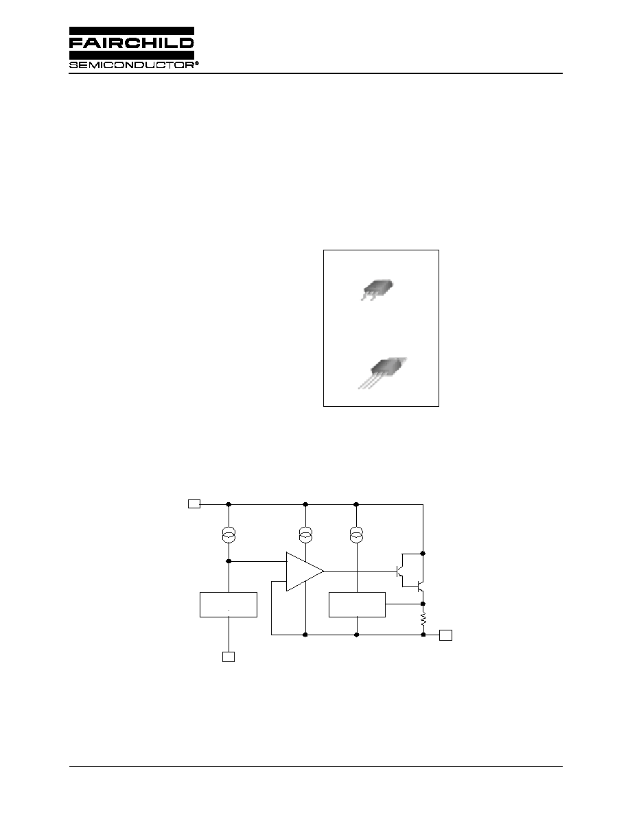
D-PAK
1. Adj 2. Output 3. Input
1
2
3
TO-220
1 2 3
Internal Block Diagram
R limit
3
V in
V o
1
V olta ge
Re fe re nce
V ad j
2
P rotection
Circ uitry
+
-
Input
Output
KA317M
3-Terminal 0.5A Positive Adjustable Regulator
KA317M
2
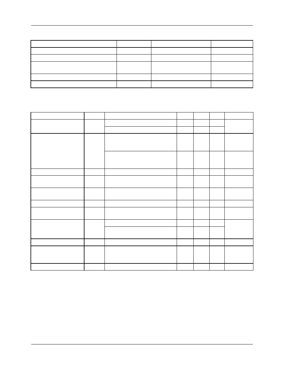
Absolute Maximum Ratings
Electrical Characteristics
(V
I
-V
O
=5V, I
O
= 0.1A, 0
°
C
T
J
+ 125
°
C,
P
DMAX
= 7.5W, unless otherwise specified)
Note :
1. Thermal resistance test board
Size: 76.2mm * 114.3mm * 1.6mm(1S0P)
JEDEC standard: JESD51-3, JESD51-7
2. Assume no ambient airflow.
3. Load and Line regulation are specified at constant junction temperature. Change in V
O
due to heating effects must be taken
into account separately. Pulse testing with low duty cycle is used.
4. C
ADJ
, when used, is connected between the adjustment pin and ground.
Parameter
Symbol
Value
Unit
Input Output Voltage Differential
V
I
- V
O
40
V
Power Dissipation
P
D
Internally limited
W
Thermal Resistance Junction-Air
D-PAK (Note1,2)
R
JA
100
°
C/W
Operating Junction Temperature Range
T
j
0 ~ +125
°
C
Storage Temperature Range
T
STG
-65 ~+125
°
C
Parameter
Symbol
Conditions
Min.
Typ.
Max.
Unit
Line Regulation (Note3)
Rline
T
A
= +25
°
C, 3V
V
I
-
V
O
40V
-
0.01
0.04
%/ V
3V
V
I
-
V
O
40V
-
0.02
0.07
Load Regulation (Note3)
Rload
T
A
=+ 25
°
C, 10mA
I
O
0.5A
V
O
5V
V
O
5V
-
5
0.1
25
0.5
mV
%/ V
O
10mA
I
O
0.5A
V
O
5V
V
O
5V
-
20
0.3
70
1.5
mV
%/ V
O
Adjustment Pin Current
I
ADJ
-
-
50
100
uA
Adjustment Pin Current
Change
I
ADJ
3V
V
I
- V
O
40V
10mA
I
O
0.5A, P
D
<
P
DMAX
-
0.2
5
uA
Reference Voltage
V
REF
3V
<
V
I
- V
O
<
40V
10mA
I
O
0.5A, P
D
<
P
DMAX
1.20
1.25
1.30
V
Temperature Stability
ST
T
-
-
0.7
-
%/ V
O
Minimum Load Current to
Maintain Regulation
I
L(MIN)
V
I
- V
O
=
40V
-
3.5
10
mA
Maximum Output Current I
O(MAX)
V
I
- V
O
15V, P
D
<
P
DMAX
0.5
0.9
-
A
V
I
- V
O
=
40V
P
D
<
P
DMAX
, T
A
=+ 25
°
C
0.15
0.25
-
RMS Noise, % of V
OUT
e
N
T
A
= +25
°
C, 10Hz
<
f
<
10KHz
-
0.003
-
%/ V
O
Ripple Rejection
RR
V
O
= 10V, f = 120Hz
without C
ADJ
C
ADJ
= 10uF (Note4)
66
65
80
-
dB
Long-Term Stability
ST
T
J
=+ 125
°
C, 1000Hours
-
0.3
1
%/1000Hrs

KA317M
3
Typical Performance Characteristics
Figure 1. Minimum Load Current
Figure 2. Peak Output Current vs. Input-Output
Differential Voltage
Figure 3. Adjustment Pin Current vs. Temperature
Figure 4. Ripple Rejection vs. Frequency
Figure 5. Load Regulation vs. Temperature
Figure 6. Line Regulation vs. Temperature

KA317M
4
Typical Performance Characteristics
(Continued)
Figure 7. Outputvoltage vs. Temperature
Figure 8. Thermal Shutdown

KA317M
5
Typical Application
Figure 1. 15V Electronic Shutdown Regulator
D1 protects the device during an input short circuit.
Figure 2. Slow Turn-On Regulator
Figure 3. Current Regulator
Input
Output
Input
Output
Input
Output
KA317M
6
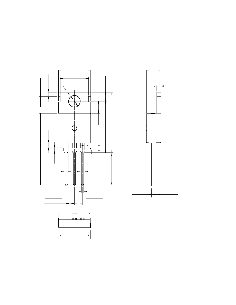
Mechanical Dimensions
Package
Dimensions in millimeters
4.50
±
0.20
9.90
±
0.20
1.52
±
0.10
0.80
±
0.10
2.40
±
0.20
10.00
±
0.20
1.27
±
0.10
ř3.60
±
0.10
(8.70)
2.80
±
0.10
15.90
±
0.20
10.08
±
0.30
18.95MAX.
(1.70)
(3.70)
(3.00)
(1.46)
(1.00)
(45
°
)
9.20
±
0.20
13.08
±
0.20
1.30
±
0.10
1.30
+0.10
0.05
0.50
+0.10
0.05
2.54TYP
[2.54
±
0.20
]
2.54TYP
[2.54
±
0.20
]
TO-220

KA317M
7
Mechanical Dimensions
(Continued)
Package
Dimensions in millimeters
6.60
±
0.20
2.30
±
0.10
0.50
±
0.10
5.34
±
0.30
0.70
±
0.20
0.60
±
0.20
0.80
±
0.20
9.50
±
0.30
6.10
±
0.20
2.70
±
0.20
9.50
±
0.30
6.10
±
0.20
2.70
±
0.20
MIN0.55
0.76
±
0.10
0.50
±
0.10
1.02
±
0.20
2.30
±
0.20
6.60
±
0.20
0.76
±
0.10
(5.34)
(1.50)
(2XR0.25)
(5.04)
0.89
±
0.10
(0.10)
(3.05)
(1.00)
(0.90)
(0.70)
0.91
±
0.10
2.30TYP
[2.30
±
0.20]
2.30TYP
[2.30
±
0.20]
MAX0.96
(4.34)
(0.50)
(0.50)
D-PAK
KA317M
3/14/02 0.0m 001
Stock#DSxxxxxxxx
2002 Fairchild Semiconductor Corporation
LIFE SUPPORT POLICY
FAIRCHILD'S PRODUCTS ARE NOT AUTHORIZED FOR USE AS CRITICAL COMPONENTS IN LIFE SUPPORT DEVICES
OR SYSTEMS WITHOUT THE EXPRESS WRITTEN APPROVAL OF THE PRESIDENT OF FAIRCHILD SEMICONDUCTOR
CORPORATION. As used herein:
1. Life support devices or systems are devices or systems
which, (a) are intended for surgical implant into the body,
or (b) support or sustain life, and (c) whose failure to
perform when properly used in accordance with
instructions for use provided in the labeling, can be
reasonably expected to result in a significant injury of the
user.
2. A critical component in any component of a life support
device or system whose failure to perform can be
reasonably expected to cause the failure of the life support
device or system, or to affect its safety or effectiveness.
www.fairchildsemi.com
DISCLAIMER
FAIRCHILD SEMICONDUCTOR RESERVES THE RIGHT TO MAKE CHANGES WITHOUT FURTHER NOTICE TO ANY
PRODUCTS HEREIN TO IMPROVE RELIABILITY, FUNCTION OR DESIGN. FAIRCHILD DOES NOT ASSUME ANY
LIABILITY ARISING OUT OF THE APPLICATION OR USE OF ANY PRODUCT OR CIRCUIT DESCRIBED HEREIN; NEITHER
DOES IT CONVEY ANY LICENSE UNDER ITS PATENT RIGHTS, NOR THE RIGHTS OF OTHERS.
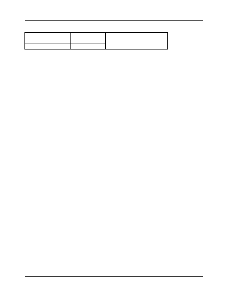
Ordering Information
Product Number
Package
Operating Temperature
KA317M
TO-220
0 ~ 125
°
C
KA317MR
D-PAK