Äîêóìåíòàöèÿ è îïèñàíèÿ www.docs.chipfind.ru
SPS
KA1M0880
1
#3 V
CC
32V
5
µ
A
5V
2.5R
1R
1mA
0.1V
+
-
OVER VOLTAGE S/D
+
-
7.5V
25V
Thermal S/D
S
R
Q
Power on reset
+
-
L.E.B
S
R
Q
OSC
5V
Vref
Internal
bias
Good
logic
SFET
#1 DRAIN
#2 GND
#4 FB
#5 Soft Start
9V
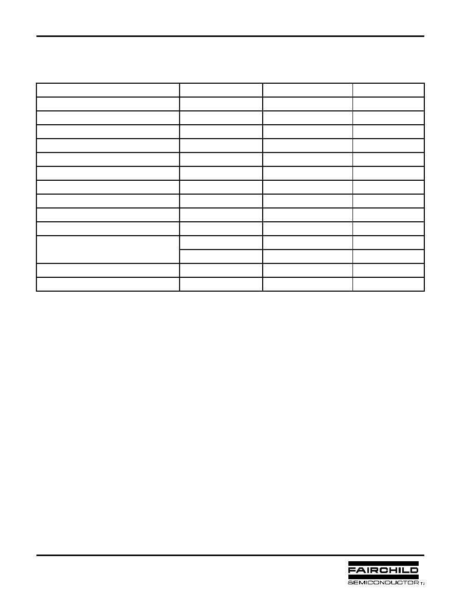
SPS
The SPS product family is specially designed for an off-line
SMPS with minimal external components. The SPS consist of
high voltage power SenseFET and current mode PWM IC.
Included PWM controller features integrated fixed oscillator,
under voltage lock out, leading edge blanking, optimized gate
turn-on/turn-off driver, thermal shut down protection, over
voltage protection, and temperature compensated precision
current sources for loop compensation and fault protection
circuitry. Compared to discrete MOSFET and controller or
RCC switching converter solution, a SPS can reduce total
component count, design size, weight and at the same time
increase efficiency, productivity, and system reliability. It has
a basic platform well suited for cost effective design in either
a flyback converter or a forward converter.
FEATURES
·
Precision fixed operating frequency (70kHz)
·
Pulse by pulse over current limiting
·
Over Current Protection
·
Over Voltage Protection (Min. 23V)
·
Internal thermal shutdown function
·
Under voltage lockout
·
Internal high voltage sense FET
·
Latch up mode
·
Soft start
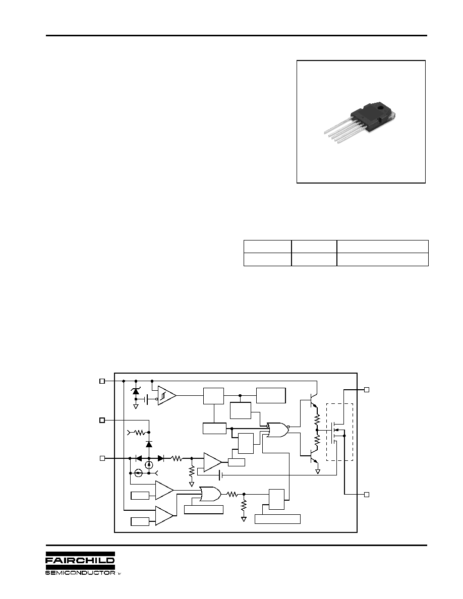
ORDERING INFORMATION
Device
Package
Operating Temperature
KA1M0880
TO-3P-5L
-
25
°
C to +85
°
C
TO-3P-5L
1.DRAIN 2. GND 3. V
CC
4. FB 5. S/S
BLOCK DIAGRAM
Rev. B
©
1999 Fairchild Semiconductor Corporation
KA1M0880
SPS
2
ABSOLUTE MAXIMUM RATINGS
NOTES:
1.
Tj=25
°
C to 150
°
C
2.
Repetitive rating: Pulse width limited by maximum junction temperature
3.
L=24mH, V
DD
=50V, R
G
=25
, starting Tj=25
°
C
Characteristic
Symbol
Value
Unit
Drain-source (GND) voltage
(1)
V
DSS
800
V
Drain-Gate voltage (R
GS
=1M
)
V
DGR
800
V
Gate-source (GND) voltage
V
GS
±
30
V
Drain current pulsed
(2)
I
DM
32.0
A
DC
Single pulsed avalanche energy
(3)
E
AS
810
mJ
Avalanche current
(4)
I
AS
-
A
Continuous drain current (T
C
=25
°
C)
I
D
8.0
A
DC
Continuous drain current (T
C
=100
°
C)
I
D
5.6
A
DC
Supply voltage
V
CC
30
V
Analog input voltage range
V
FB
-
0.3 to V
SD
V
Total power dissipation
P
D
(watt H/S)
190
W
Derating
1.54
W/
°
C
Operating temperature
T
OPR
-
25 to +85
°
C
Storage temperature
T
STG
-
55 to +150
°
C
SPS
KA1M0880
3
NOTE: Pulse test: Pulse width
300
µ
S, duty cycle
2%
ELECTRICAL CHARACTERISTICS (SFET part)
(Ta=25
°
C unless otherwise specified)
Characteristic
Symbol
Test condition
Min.
Typ.
Max.
Unit
Drain-source breakdown voltage
BV
DSS
V
GS
=0V, I
D
=50
µ
A
800
-
-
V
Zero gate voltage drain current
I
DSS
V
DS
=Max., Rating, V
GS
=0V
-
-
50
µ
A
V
DS
=0.8Max., Rating,
V
GS
=0V, T
C
=125
°
C
-
-
200
µ
A
Static drain-source on resistance
(note)
R
DS(ON)
V
GS
=10V, I
D
=5.0A
-
1.2
1.5
Forward transconductance
(note)
gfs
V
DS
=15V, I
D
=5.0A
1.5
2.5
-
mho
Input capacitance
Ciss
V
GS
=0V, V
DS
=25V,
f=1MHz
-
2460
-
pF
Output capacitance
Coss
-
210
-
Reverse transfer capacitance
Crss
-
64
-
Turn on delay time
td(on)
V
DD
=0.5BV
DSS
, I
D
=8.0A
(MOSFET switching
time are essentially
independent of
operating temperature)
-
-
90
nS
Rise time
tr
-
95
200
Turn off delay time
td(off)
-
150
450
Fall time
tf
-
60
150
Total gate charge
(gate-source+gate-drain)
Qg
V
GS
=10V, I
D
=8.0A,
V
DS
=0.5BV
DSS
(MOSFET
switching time are
essentially independent of
operating temperature)
-
-
150
nC
Gate-source charge
Qgs
-
20
-
Gate-drain (Miller) charge
Qgd
-
70
-
KA1M0880
SPS
4
NOTES:
1.
These parameters, although guaranteed, are not 100% tested in production
2.
These parameters, although guaranteed, are tested in EDS (wafer test) process
ELECTRICAL CHARACTERISTICS (Control part)
(Ta=25
°
C unless otherwise specified)
Characteristic
Symbol
Test condition
Min.
Typ.
Max.
Unit
REFERENCE SECTION
Output voltage
(1)
Vref
Ta=25
°
C
4.80
5.00
5.20
V
Temperature Stability
(1)(2)
Vref/
T
-
25
°
C
Ta
+85
°
C
-
0.3
0.6
mV/
°
C
OSCILLATOR SECTION
Initial accuracy
F
OSC
Ta=25
°
C
61
67
73
kHz
Frequency change with temperature
(2)
F/
T
-
25
°
C
Ta
+85
°
C
-
±
5
±
10
%
PWM SECTION
Maximum duty cycle
Dmax
-
74
77
80
%
FEEDBACK SECTION
Feedback source current
I
FB
Ta=25
°
C, 0V
Vfb
3V
0.7
0.9
1.1
mA
Shutdown delay current
Idelay
Ta=25
°
C, 5V
Vfb
V
SD
4.0
5.0
6.0
µ
A
OVER CURRENT PROTECTION SECTION
Over current protection
I
L
(max)
Max. inductor current
4.40
5.00
5.60
A
UVLO SECTION
Start threshold voltage
Vth(H)
-
14
15
16
V
Minimum operating voltage
Vth(L)
After turn on
9
10
11
V
TOTAL STANDBY CURRENT SECTION
Start current
I
ST
V
CC
=14V
0.1
0.3
0.45
mA
Operating supply current
(control part only)
I
OPR
Ta=25
°
C
6
12
18
mA
V
CC
zener voltage
V
Z
I
CC
=20mA
30
32.5
35
V
SHUTDOWN SECTION
Shutdown Feedback voltage
V
SD
-
6.9
7.5
8.1
V
Thermal shutdown temperature (Tj)
(1)
T
SD
-
140
160
-
°
C
Over voltage protection voltage
V
OVP
-
23
25
28
V
SPS
KA1M0880
5
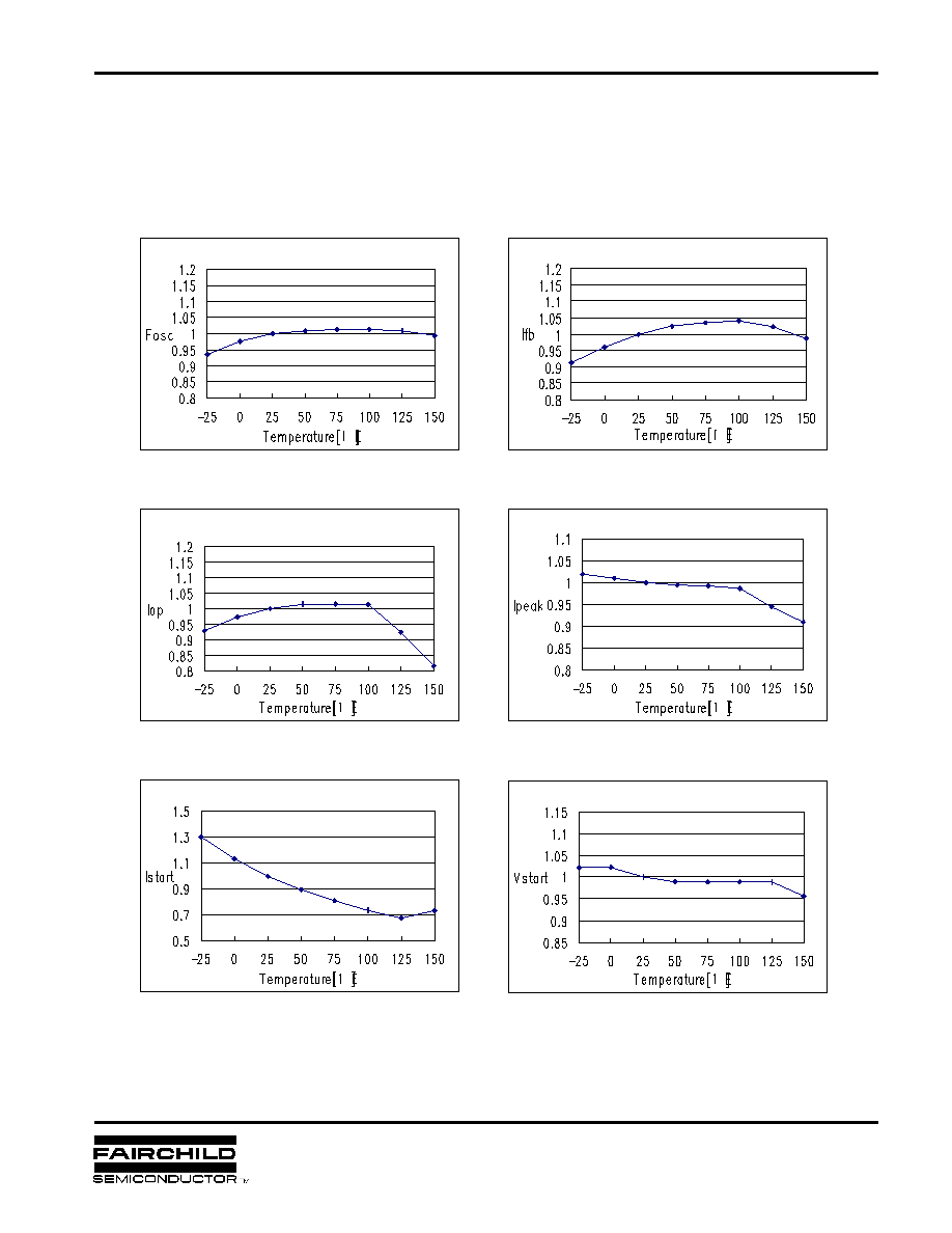
TYPICAL PERFORMANCE CHARACTERISTICS
(These characteristic graphs are normalized at Ta=25
°
C)
Figure 1. Operating Frequency
Figure 2. Feedback Source Current
Figure 3. Operating Current
Figure 4. Max. Inductor Current
Figure 5. Start up Current
Figure 6. Start Threshold Voltage
KA1M0880
SPS
6
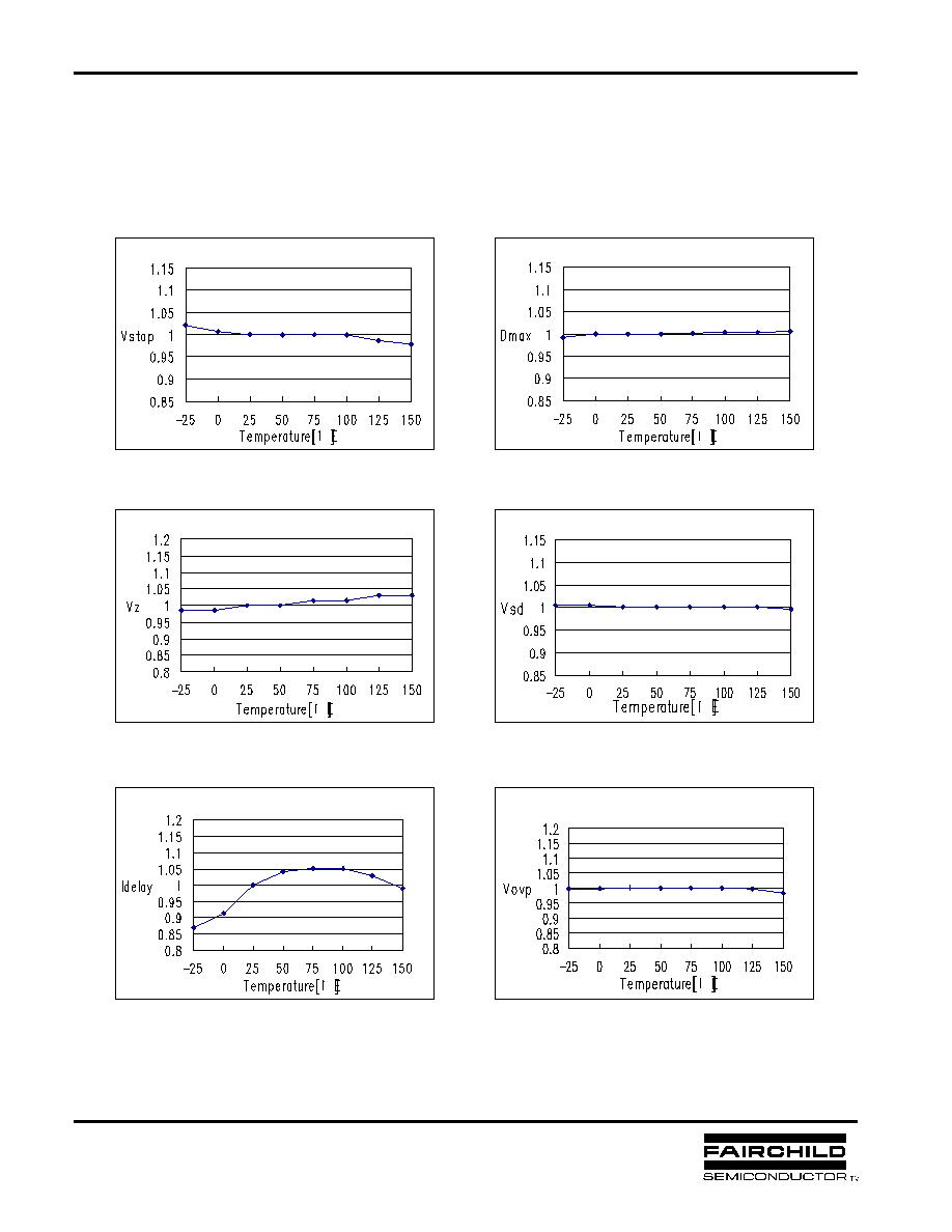
TYPICAL PERFORMANCE CHARACTERISTICS (Continued)
(These characteristic graphs are normalized at Ta=25
°
C)
Figure 7. Stop Threshold Voltage
Figure 8. Maximum Duty Cycle
Figure 9. V
CC
Zener Voltage
Figure 10. Shutdown Feedback Voltage
Figure 11. Shutdown Delay Current
Figure 12. Over Voltage Protection
SPS
KA1M0880
7
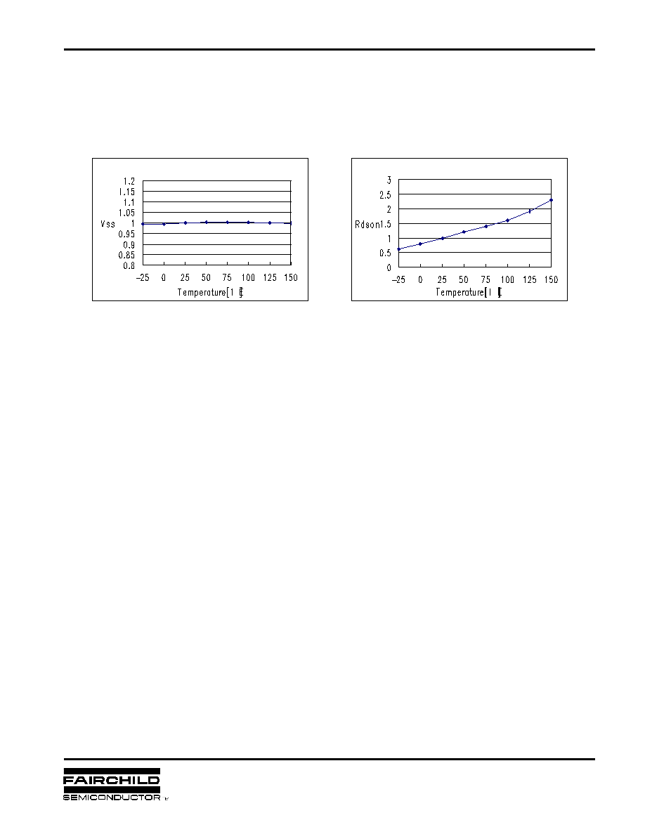
TYPICAL PERFORMANCE CHARACTERISTICS (Continued)
(These characteristic grahps are normalized at Ta=25
°
C)
Figure 13. Soft Start Voltage
Figure 14. Drain Source Turn-on Resistance

TRADEMARKS
ACExTM
CoolFETTM
CROSSVOLTTM
E
2
CMOS
TM
FACTTM
FACT Quiet SeriesTM
FAST
®
FASTrTM
GTOTM
HiSeCTM
The following are registered and unregistered trademarks Fairchild Semiconductor owns or is authorized to use and is
not intended to be an exhaustive list of all such trademarks.
LIFE SUPPORT POLICY
FAIRCHILD'S PRODUCTS ARE NOT AUTHORIZED FOR USE AS CRITICAL COMPONENTS IN LIFE SUPPORT
DEVICES OR SYSTEMS WITHOUT THE EXPRESS WRITTEN APPROVAL OF FAIRCHILD SEMICONDUCTOR CORPORATION.
As used herein:
ISOPLANARTM
MICROWIRETM
POPTM
PowerTrenchTM
QSTM
Quiet SeriesTM
SuperSOTTM-3
SuperSOTTM-6
SuperSOTTM-8
TinyLogicTM
1. Life support devices or systems are devices or
systems which, (a) are intended for surgical implant into
the body, or (b) support or sustain life, or (c) whose
failure to perform when properly used in accordance
with instructions for use provided in the labeling, can be
reasonably expected to result in significant injury to the
user.
2. A critical component is any component of a life
support device or system whose failure to perform can
be reasonably expected to cause the failure of the life
support device or system, or to affect its safety or
effectiveness.
PRODUCT STATUS DEFINITIONS
Definition of Terms
Datasheet Identification
Product Status
Definition
Advance Information
Preliminary
No Identification Needed
Obsolete
This datasheet contains the design specifications for
product development. Specifications may change in
any manner without notice.
This datasheet contains preliminary data, and
supplementary data will be published at a later date.
Fairchild Semiconductor reserves the right to make
changes at any time without notice in order to improve
design.
This datasheet contains final specifications. Fairchild
Semiconductor reserves the right to make changes at
any time without notice in order to improve design.
This datasheet contains specifications on a product
that has been discontinued by Fairchild semiconductor.
The datasheet is printed for reference information only.
Formative or
In Design
First Production
Full Production
Not In Production
DISCLAIMER
FAIRCHILD SEMICONDUCTOR RESERVES THE RIGHT TO MAKE CHANGES WITHOUT FURTHER
NOTICE TO ANY PRODUCTS HEREIN TO IMPROVE RELIABILITY, FUNCTION OR DESIGN. FAIRCHILD
DOES NOT ASSUME ANY LIABILITY ARISING OUT OF THE APPLICATION OR USE OF ANY PRODUCT
OR CIRCUIT DESCRIBED HEREIN; NEITHER DOES IT CONVEY ANY LICENSE UNDER ITS PATENT
RIGHTS, NOR THE RIGHTS OF OTHERS.
UHCTM
VCXTM
Document Outline
- Main Menu
- Analog & Mixed Signal
- SPS PSG
- SPS Index
- Search
- fairchildsemi.com