©2001 Fairchild Semiconductor Corporation
www.fairchildsemi.com
Rev.1.0.4
Features
· Single Chip 650V 1A SenseFET PowerSwitch
· Precision Fixed Operating Frequency (100kHz)
· Internal Start-up Switch
· UVLO with Hysterisis (6.7V/8.7V)
· Over Load Protection (typ. 4.5V)
· Over Current Protection (typ. 0.6A)
· Internal Thermal Shutdown Function
· Secondary Side Regulation
· Auto-restart mode
· No load consumption <250mW at 265VAC input
Applications
· Charger & Adaptor for Mobile Phone, PDA & MP3
· Auxiliary Power for PC
Description
The FSDH0165 is specially designed for an off-line SMPS with
minimal external components. The FSDH0165 is a monolithic
high voltage power switching regulator that combine the
SenseFET(LDMOS) with voltage mode PWM control block.
Included PWM controller features integrated fixed oscillator,
under voltage lock out, leading edge blanking, optimized gate
turn-on/turn-off driver, thermal shut down protection and
temperature compensated precision current sources for loop
compensation and fault protection circuitry. compared to
discrete MOSFET and controller or R
CC
switching converter
solution, a FSDH0165 can reduce total component count,
design size, weight and at the same time increase efficiency,
productivity, and system reliability. It has a basic platform well
suited for cost effective design in a flyback converter.
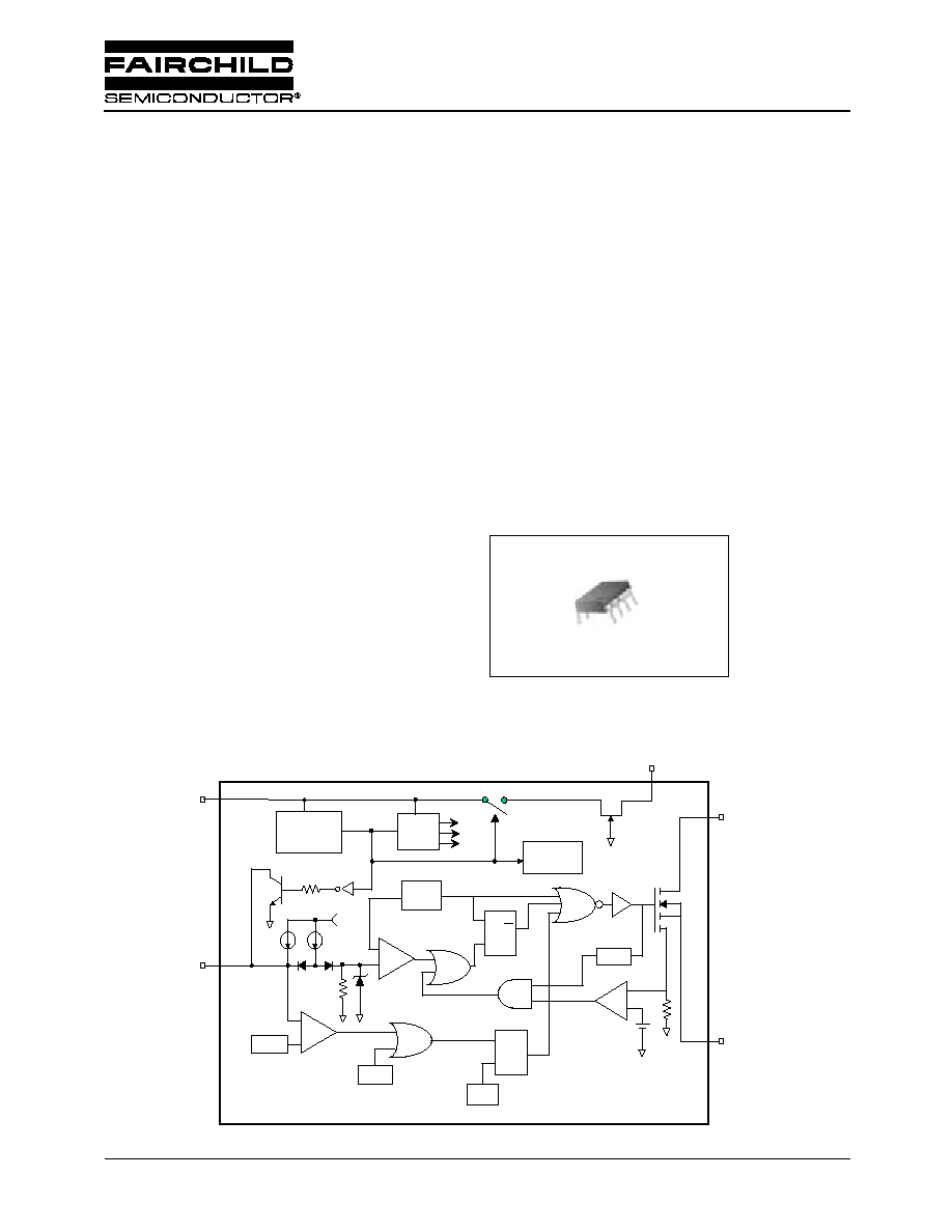
1.Vstr 2.Vfb 3.4.5.6.GND 7.Vcc 8.Drain
8-DIPH
1
Internal Block Diagram
FSDH0165
Fairchild Power Switch(FPS)
#8 : Drain
#3,#4,#5,#6
GND
#7 : Vcc
#2 : Vfb
SFET
4.5V
VREF
OSC
INTERNAL
BIAS
_
+
5.8V
0.45 mA
5 uA
+
_
4.5V
TSD
Q
S
R
÷4
L.E.B
_
+
Vth
UVLO
VREG(5.8V)
Q
S
R
#1 : Vstr
OLP
PWM
OCP
UVLO 8.7V
UVLO 6.7V
#8 : Drain
#3,#4,#5,#6
GND
#7 : Vcc
#2 : Vfb
SFET
4.5V
VREF
OSC
INTERNAL
BIAS
_
+
_
+
5.8V
0.45 mA
5 uA
+
_
+
_
4.5V
TSD
Q
S
R
÷4
L.E.B
_
+
_
+
Vth
UVLO
VREG(5.8V)
Q
S
R
#1 : Vstr
OLP
PWM
OCP
UVLO 8.7V
UVLO 6.7V

FSDH0165
2
Absolute Maximum Ratings
(Ta=25
°
C unless otherwise specified)
PIN Definitions
Parameter
Symbol
Value
Unit
Maximum Drain Voltage
V
D,MAX
650
V
Continuous Drain Current (T
C
=25
°
C)
I
D
0.6
A
DC
Maximum Supply Voltage
V
CC,MAX
21
V
Input Voltage Range
V
FB
-
0.3 to V
SD
V
Operating Ambient Temperature
T
A
-
25 to +85
°
C
Storage Temperature Range
T
STG
-
55 to +150
°
C
Pin Number
Pin Name
Pin Function Description
1
Vstr
This pin connects directly to the rectified AC line voltage source. At start up
the internal switch supplies internal bias and charges an external capacitor
that connects from the Vcc pin to ground. once this reaches 8.7V, Vstr is
isolated internally.
2
Vfb
This pin is the inverting input of the PWM comparator, and it operates
normally between 0.5V and 2.5V. It has a 0.45mA current source
connected internally and a capacitor and opto coupler connected
externally. A feedback voltage of 3.5V to 4.5V triggers overload protection
(OLP). There is a time delay due to the 5uA current source, which prevents
false triggering under transient conditions but still allows the protection
mechanism to operate under true overload conditions.
3,4,5,6
GND
These pins are the control ground and the SenseFET Source.
7
Vcc
This is the positive supply voltage input. During start up, power is supplied
to this input from Pin 1. When Vcc reaches the UVLO upper threshold
(8.7V), the start up Internal Switch (Vstr) turns off and power is supplied
from auxiliary transformer winding.
8
Drain
This pin is designed to directly drive the converter transformer and is
capable of switching a maximum of 650V and 1A.
FSDH0165
3
Electrical Characteristics
(Ta=25
°
C unless otherwise specified)
Note:
1.These parameters, although guaranteed, are not 100% tested in production
Parameter
Symbol
Condition
Min.
Typ.
Max.
Unit
SENSEFET SECTION
Drain-Source Breakdown Voltage
BV
DSS
V
GS
= 0V, I
D
= 100
µ
A
650
-
-
V
Zero gate voltage drain current
I
DSS
V
DS
= 520V
-
-
100
µ
A
Static drain-source on Resistance
R
DS(ON)
I
D
= 50mA Tj = 25
°
C
-
15.6
18
I
D
= 50mA Tj = 100
°
C
-
25.7
30
Rise Time
T
R
V
DS
= 325V, I
D
= 300mA
-
100
-
nS
Fall Time
T
F
V
DS
= 325V, l
D
= 50mA
-
50
-
nS
START UP SECTION
VSTR Supply Voltage
V
ST
-
17
-
-
V
UVLO SECTION
Start Threshold Voltage
Vstart
-
8.0
8.7
9.4
V
Stop Threshold Voltage
Vstop
After turn on
6.0
6.7
7.4
V
OSCILLATOR SECTION
Initial accuracy
F
OSC
Tj = 25
°
C
90
100
110
kHz
Maximum Duty Cycle
Dmax
Vfb = 3V
64
67
70
%
Minimum Duty Cycle
Dmin
Vfb = 0V
-
0
0
%
FEEDBACK SECTION
Feedback Source Current
I
FB
Vfb = 0V
0.40
0.45
0.50
mA
Shutdown feedback Voltage
V
SD
-
4.0
4.5
5.0
V
CURRENT LIMIT(SELF-PROTECTION)SECTION
Peak Current Limit
I
OVER
peak inductor current
0.5
0.6
0.7
A
PROTECTION SECTION
Thermal Shutdown Temperature (Tj)
(1)
T
SD
-
125
145
-
°
C
TOTAL DEVICE SECTION
Operating Supply Current
I
OPR
V
CC
= 21V (Max)
-
-
4
mA

FSDH0165
4
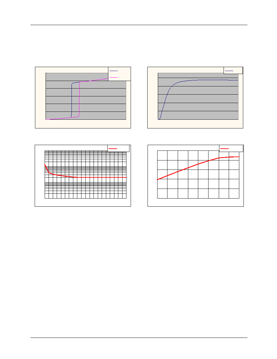
Typical Performance Characteristics
(These characteristic graphs are normalized at Ta=25
°
C)
Figure 1. Stop Threshold Voltage
Figure 2. Start Threshold Voltage
Figure 3. Operating Supply Current
Figure 4. Feedback Source Current
Figure 5. Initial Accuracy
Figure 6. Peak Current Limit
6.7
6.8
6.9
7
7.1
7.2
-25
0
25
50
75
100
125
150 [°C]
[V]
Vstop
8.76
8.8
8.84
8.88
8.92
8.96
-25
0
25
50
75
100
125
150 [°C]
[V]
Vstart
2.1
2.15
2.2
2.25
2.3
2.35
2.4
-25
0
25
50
75
100
125
150[°C]
[mA]
Iopr
0.38
0.4
0.42
0.44
0.46
-25
0
25
50
75
100
125
150 [°C]
[A]
Ifb
84
88
92
96
100
104
108
-25
-10
0
25
50
75
100
125
150[°C]
[kHz]
Fosc
0.2
0.3
0.4
0.5
0.6
0.7
0.8
-25
-10
0
25
50
75
100
125
150[°C]
[A]
Ipeak
FSDH0165
5
Typical Performance Characteristics
(Continued)
(These characteristic graphs are normalized at Ta=25
°
C)
Figure 7. Stop/Start Threshold Voltage
Figure 8. VSTR Supply Voltage
0.00
0.50
1.00
1.50
2.00
2.50
3.00
0
2.5
5
7.5
10
12.5
15
17.5
20[V]
[mA]
Vstop
Vstart
0.00
0.50
1.00
1.50
2.00
2.50
1
13
25
37
49
61
73
85
97[V]
[mA]
Vstr
1
10
100
1000
0
25
50
75
100
[V]
[pF]
Coss
600
640
680
720
760
800
-50
0
50
100
150
[°C]
[V]
BVdss
Figure 9. Coss vs. Drain Voltage
Figure 10. Breakdown vs. Temperature