Äîêóìåíòàöèÿ è îïèñàíèÿ www.docs.chipfind.ru
February 2004
2004 Fairchild Semiconductor Corporation
FDS7288N3 Rev C1 (W)
FDS7288N3
30V N-Channel PowerTrench
MOSFET
General Description
This N-Channel MOSFET in the thermally enhanced
SO8 FLMP package has been designed specifically to
improve the overall efficiency of DC/DC converters.
Providing a balance of low R
DS(ON)
and Qg it is ideal for
synchronous rectifier applications in both isolated and
non-isolated topologies. It is also well suited for both
high and low side switch applications in Point of Load
converters.
Applications
· Secondary side Synchronous rectifier
· Synchronous Buck VRM and POL Converters
Features
· 20.5 A, 30 V R
DS(ON)
= 4.5 m
@ V
GS
= 10 V
R
DS(ON)
= 5.6 m
@ V
GS
= 4.5 V
· High performance trench technology for extremely
low R
DS(ON)
· Low Qg and Rg for fast switching
· SO-8 FLMP for enhanced thermal performance in an
industry-standard package outline.
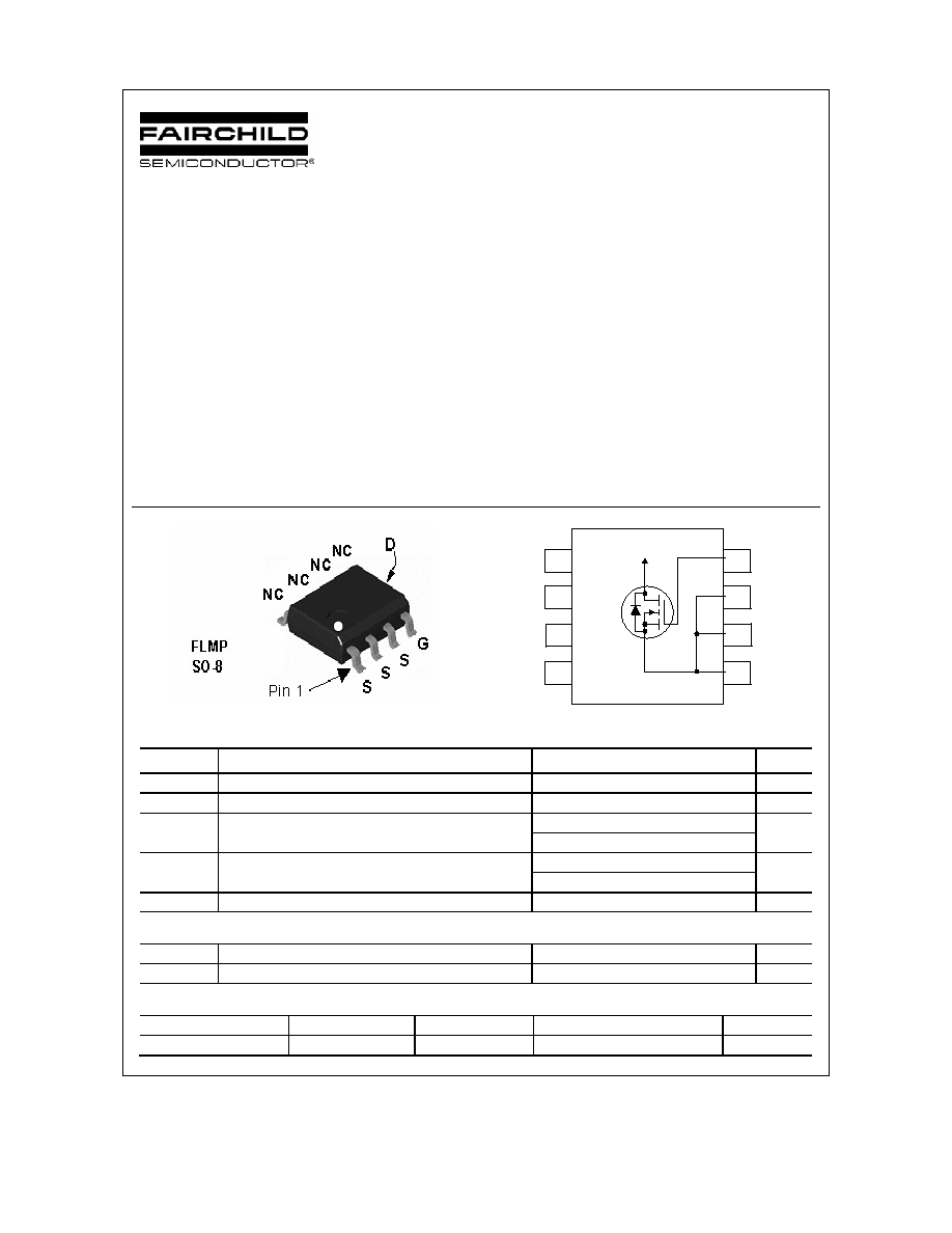
4
5
3
6
2
7
1
8
Bottom-side
Drain Contact
Absolute Maximum Ratings
T
A
=25
o
C unless otherwise noted
Symbol Parameter
Ratings
Units
V
DSS
Drain-Source Voltage
30
V
V
GSS
Gate-Source
Voltage
±20
V
I
D
Drain Current Continuous
(Note 1a)
20 A
Pulsed
60
P
D
Power Dissipation for Single Operation
(Note 1a)
3.0
(Note 1b)
1.5
W
T
J
, T
STG
Operating and Storage Junction Temperature Range
55 to +150
°C
Thermal Characteristics
R
JA
Thermal Resistance, Junction-to-Ambient
(Note 1a)
40
°C/W
R
JC
Thermal Resistance, Junction-to-Case
(Note 1)
0.5
°C/W
Package Marking and Ordering Information
Device Marking
Device
Reel Size
Tape width
Quantity
FDS7288N3
FDS7288N3
13''
12mm
2500 units
FDS7288N3
FDS7288N3 Rev C1 (W)
Electrical Characteristics
T
A
= 25°C unless otherwise noted
Symbol Parameter
Test
Conditions
Min
Typ
Max
Units
Off Characteristics
BV
DSS
DrainSource Breakdown Voltage V
GS
= 0 V, I
D
= 250
µA
30 V
BV
DSS
T
J
Breakdown Voltage Temperature
Coefficient
I
D
= 250
µA, Referenced to 25°C
25 mV/
°C
I
DSS
Zero Gate Voltage Drain Current
V
DS
= 24 V, V
GS
= 0 V
10
µA
I
GSS
GateBody
Leakage
V
GS
=
± 20 V, V
DS
= 0 V
± 100
nA
On Characteristics
(Note 2)
V
GS(th)
Gate Threshold Voltage
V
DS
= V
GS
, I
D
= 250
µA
1 1.8 3 V
V
GS(th)
T
J
Gate Threshold Voltage
Temperature Coefficient
I
D
= 250
µA, Referenced to 25°C
5 mV/
°C
R
DS(on)
Static DrainSource
OnResistance
V
GS
= 10 V, I
D
= 20.5 A
V
GS
= 4.5 V, I
D
= 18.5 A
V
GS
= 10 V, I
D
= 20.5 A,T
J
= 125
°C
3.8
4.6
5.2
4.5
5.6
7.6
m
g
FS
Forward
Transconductance V
DS
= 10 V, I
D
= 20.5 A
106
S
Dynamic Characteristics
C
iss
Input
Capacitance
3300
pF
C
oss
Output
Capacitance
845
pF
C
rss
Reverse Transfer Capacitance
V
DS
= 15 V, V
GS
= 0 V,
f = 1.0 MHz
230 pF
R
G
Gate
Resistance
V
GS
= 15 mV, f = 1.0 MHz
1.6
Switching Characteristics
(Note 2)
t
d(on)
TurnOn
Delay
Time
12
22
ns
t
r
TurnOn Rise Time
11
20
ns
t
d(off)
TurnOff Delay Time
45
72
ns
t
f
TurnOff
Fall
Time
V
DD
= 15 V, I
D
= 1 A,
V
GS
= 10 V, R
GEN
= 6
32 51 ns
Q
g
Total Gate Charge
V
DS
= 15 V, I
D
= 20.5 A, V
GS
=10 V
49 69 nC
Q
g
Total Gate Charge
26
36
nC
Q
gs
GateSource
Charge
8.8
nC
Q
gd
GateDrain
Charge
V
DS
= 15 V, I
D
= 20.5 A, V
GS
= 5 V
6.7 nC
DrainSource Diode Characteristics and Maximum Ratings
I
S
Maximum Continuous DrainSource Diode Forward Current
2.5
A
V
SD
DrainSource Diode Forward
Voltage
V
GS
= 0 V, I
S
= 2.5 A
(Note 2)
0.70
1.2 V
t
rr
Diode Reverse Recovery Time
36
nS
Q
rr
Diode Reverse Recovery Charge
I
F
= 20.5 A,
d
iF
/d
t
= 100 A/µs
25 nC
FDS7288N3
FDS7288N3 Rev C1 (W)
Notes:
1. R
JA
is the sum of the junction-to-case and case-to-ambient thermal resistance where the case thermal reference is defined as the solder mounting surface of
the drain pins. R
JC
is guaranteed by design while R
CA
is determined by the user's board design.
a) 40°C/W
when
mounted on a 1in
2
pad
of 2 oz copper
b)
85°C/W when mounted on
a minimum pad of 2 oz
copper
Scale 1 : 1 on letter size paper
2. Pulse Test: Pulse Width < 300
µs, Duty Cycle < 2.0%
FDS7288N3
FDS7288N3 Rev C1 (W)
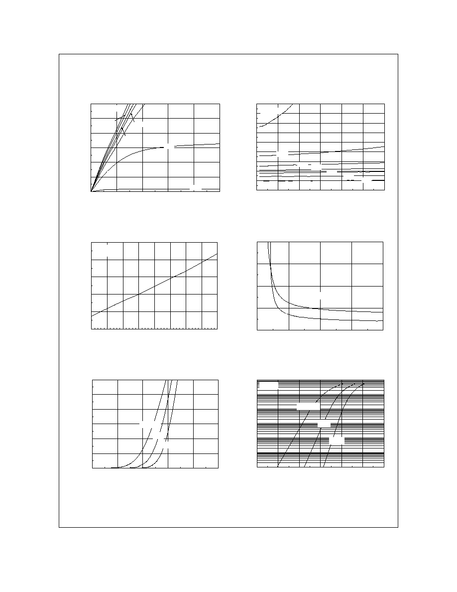
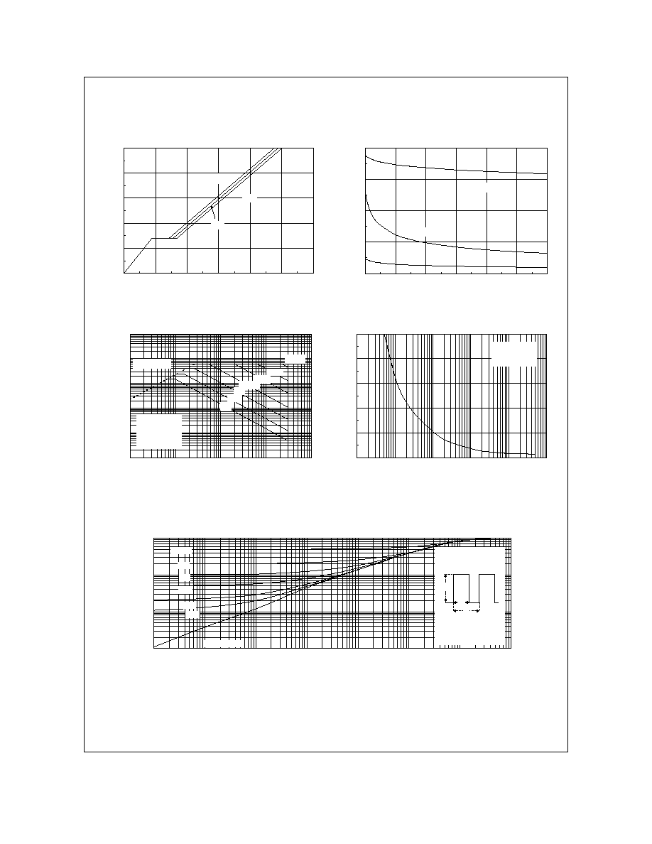
Typical Characteristics
0
10
20
30
40
50
60
0
0.2
0.4
0.6
0.8
1
V
DS
, DRAIN-SOURCE VOLTAGE (V)
I
D
,
DRA
I
N
CUR
RE
NT
(
A
)
3.5V
6.0V
V
GS
=10V
4.0V
3.0V
2.5V
4.5V
0.8
1
1.2
1.4
1.6
1.8
2
2.2
2.4
2.6
0
10
20
30
40
50
60
I
D
, DRAIN CURRENT (A)
R
DS
(O
N)
,
NO
RM
ALI
Z
ED
D
RAI
N-
SO
UR
CE O
N
-
R
ES
IS
TA
NCE
V
GS
= 3.0V
6.0V
4.0V
10V
4.5V
5.0V
3.5V
Figure 1. On-Region Characteristics.
Figure 2. On-Resistance Variation with
Drain Current and Gate Voltage.
0.6
0.8
1
1.2
1.4
1.6
-50
-25
0
25
50
75
100
125
150
T
J
, JUNCTION TEMPERATURE (
o
C)
R
DS
(O
N
)
,
NO
R
M
AL
I
Z
E
D
DR
AIN
-
SOU
R
C
E
ON-
R
ESISTAN
CE
I
D
= 20.5A
V
GS
= 10V
0.002
0.006
0.01
0.014
0.018
2
4
6
8
10
V
GS
, GATE TO SOURCE VOLTAGE (V)
R
DS(
O
N)
, ON-R
ES
IST
A
N
C
E
(OHM)
I
D
= 10.25A
T
A
= 125
o
C
T
A
= 25
o
C
Figure 3. On-Resistance Variation
withTemperature.
Figure 4. On-Resistance Variation with
Gate-to-Source Voltage.
0
10
20
30
40
50
60
1.5
2
2.5
3
3.5
4
V
GS
, GATE TO SOURCE VOLTAGE (V)
I
D
, DR
AIN CURRE
NT (A)
T
A
=125
o
C
25
o
C
-55
o
C
V
DS
= 5V
0.0001
0.001
0.01
0.1
1
10
100
0
0.2
0.4
0.6
0.8
1
1.2
V
SD
, BODY DIODE FORWARD VOLTAGE (V)
I
S
,
R
E
V
E
R
SE DRA
IN CU
RR
ENT (A
)
T
A
= 125
o
C
25
o
C
-55
o
C
V
GS
= 0V
Figure 5. Transfer Characteristics.
Figure 6. Body Diode Forward Voltage Variation
with Source Current and Temperature.
FDS7288N3
FDS7288N3 Rev C1 (W)
Typical Characteristics
0
2
4
6
8
10
0
10
20
30
40
50
60
Q
g
, GATE CHARGE (nC)
V
GS
,
G
A
TE
-S
O
URCE
VO
LT
AG
E (V
)
I
D
= 20.5A
V
DS
= 10V
20V
15V
0
1000
2000
3000
4000
0
5
10
15
20
25
30
V
DS
, DRAIN TO SOURCE VOLTAGE (V)
CA
PAC
I
T
ANC
E (p
F)
C
iss
C
rss
C
oss
f = 1MHz
V
GS
= 0 V
Figure 7. Gate Charge Characteristics.
Figure 8. Capacitance Characteristics.
0.01
0.1
1
10
100
1000
0.01
0.1
1
10
100
V
DS
, DRAIN-SOURCE VOLTAGE (V)
I
D
, DRA
IN CU
RR
ENT (
A
)
DC
1s
100ms
R
DS(ON)
LIMIT
V
GS
= 10V
SINGLE PULSE
R
JA
= 85
o
C/W
T
A
= 25
o
C
10ms
1ms
100µs
10s
0
10
20
30
40
50
0.01
0.1
1
10
100
1000
t
1
, TIME (sec)
P(pk)
,
PEA
K TRA
N
SIEN
T
PO
W
E
R
(W)
SINGLE PULSE
R
JA
= 85°C/W
T
A
= 25°C
Figure 9. Maximum Safe Operating Area.
Figure 10. Single Pulse Maximum
Power Dissipation.
0.001
0.01
0.1
1
0.0001
0.001
0.01
0.1
1
10
100
1000
t
1
, TIME (sec)
r
(
t
)
,
NO
R
M
AL
I
Z
E
D
EF
F
E
CT
I
V
E
T
R
ANS
I
E
N
T
T
H
ERM
A
L R
E
S
I
STANC
E
R
JA
(t) = r(t) * R
JA
R
JA
= 85 °C/W
T
J
- T
A
= P * R
JA
(t)
Duty Cycle, D = t
1
/ t
2
P(pk)
t
1
t
2
SINGLE PULSE
0.01
0.02
0.05
0.1
0.2
D = 0.5
Figure 11. Transient Thermal Response Curve.
Thermal characterization performed using the conditions described in Note 1b.
Transient thermal response will change depending on the circuit board design.
FDS7288N3