January 2004
2004 Fairchild Semiconductor Corporation
FDS7064N Rev C2 (W)
FDS7064N
30V N-Channel PowerTrench
MOSFET
General Description
This N-Channel MOSFET has been designed
specifically to improve the overall efficiency of DC/DC
converters using either synchronous or conventional
switching PWM controllers. It has been optimized for
"low side" synchronous rectifier operation, providing an
extremely low R
DS(ON)
in a small package.
Applications
· Synchronous rectifier
· DC/DC converter
Features
· 16 A, 30 V
R
DS(ON)
= 7.5 m
@ V
GS
= 4.5 V
· High performance trench technology for extremely
low R
DS(ON)
· High power and current handling capability
· Fast switching
· FLMP SO-8 package: Enhanced thermal
performance in industry-standard package size
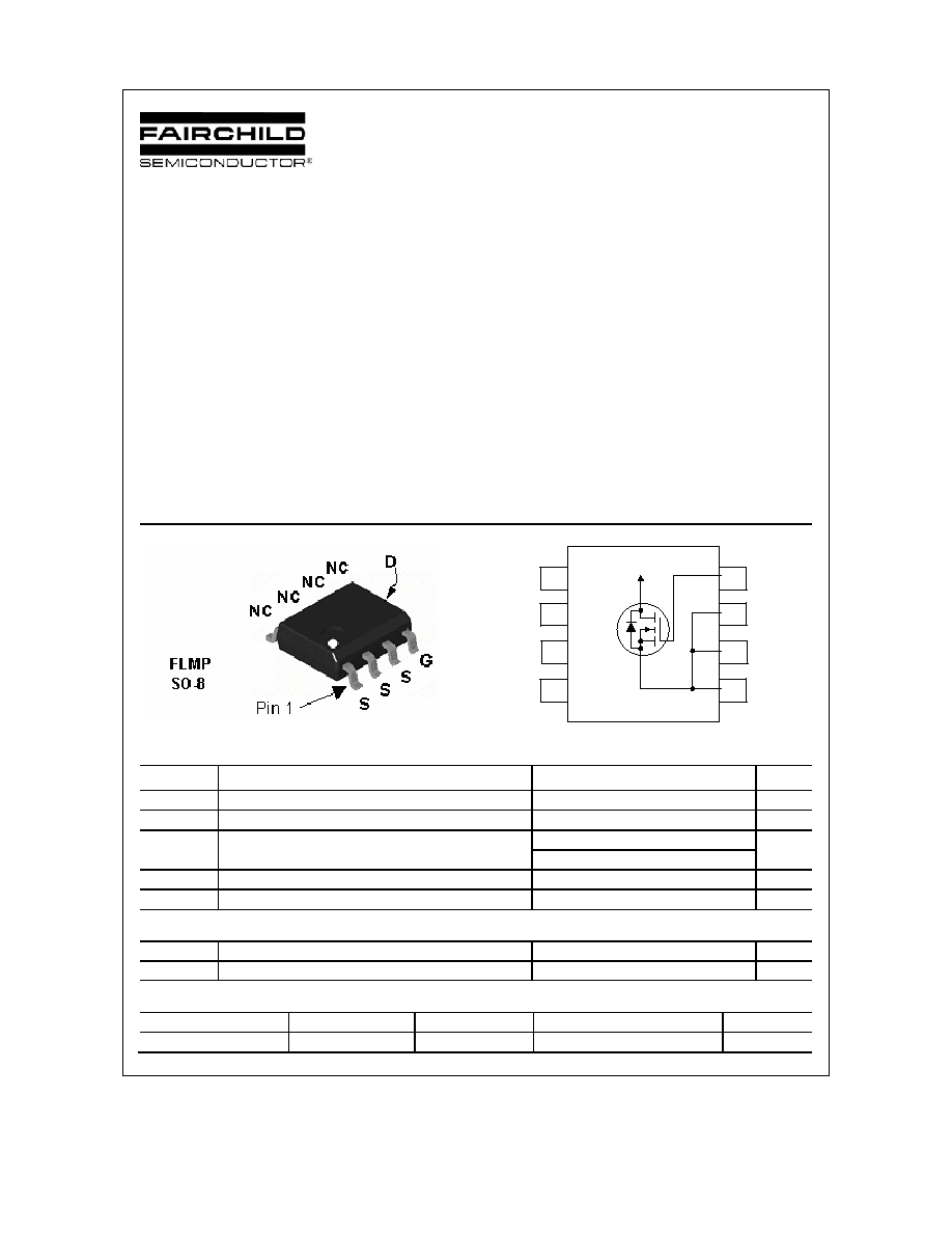
4
5
3
6
2
7
1
8
Bottom-side
Drain Contact
Absolute Maximum Ratings
T
A
=25
o
C unless otherwise noted
Symbol Parameter
Ratings
Units
V
DSS
Drain-Source Voltage
30
V
V
GSS
Gate-Source
Voltage
± 12
V
I
D
Drain Current Continuous
(Note 1a)
16 A
Pulsed
60
P
D
Power Dissipation for Single Operation
(Note 1a)
3.0 W
T
J
, T
STG
Operating and Storage Junction Temperature Range
55 to +150
°C
Thermal Characteristics
R
JA
Thermal Resistance, Junction-to-Ambient
(Note 1a)
40
°C/W
R
JC
Thermal Resistance, Junction-to-Case
0.5
°C/W
Package Marking and Ordering Information
Device Marking
Device
Reel Size
Tape width
Quantity
FDS7064N
FDS7064N
13''
12mm
2500 units
FDS7064N

FDS7064N Rev C2 (W)
Electrical Characteristics
T
A
= 25°C unless otherwise noted
Symbol Parameter
Test
Conditions
Min
Typ
Max
Units
Off Characteristics
BV
DSS
DrainSource Breakdown Voltage V
GS
= 0 V, I
D
= 250
µA
30 V
BV
DSS
T
J
Breakdown Voltage Temperature
Coefficient
I
D
= 250
µA, Referenced to 25°C
23 mV/
°C
I
DSS
Zero Gate Voltage Drain Current
V
DS
= 24 V, V
GS
= 0 V
1
µA
I
GSSF
GateBody Leakage, Forward
V
GS
= 12 V, V
DS
= 0 V
100
nA
I
GSSR
GateBody Leakage, Reverse
V
GS
= 12 V , V
DS
= 0 V
100
nA
On Characteristics
(Note 2)
V
GS(th)
Gate Threshold Voltage
V
DS
= V
GS
, I
D
= 250
µA
0.8 1.2 2
V
V
GS(th)
T
J
Gate Threshold Voltage
Temperature Coefficient
I
D
= 250
µA, Referenced to 25°C
4.3 mV/
°C
R
DS(on)
Static DrainSource
OnResistance
V
GS
= 4.5 V, I
D
= 16 A
V
GS
= 4.5 V, I
D
= 16 A,T
J
= 125
°C
6.2
9.0
7.5
11.0
m
g
FS
Forward
Transconductance V
DS
= 5 V, I
D
= 16 A
112
S
Dynamic Characteristics
C
iss
Input
Capacitance
3355
pF
C
oss
Output Capacitance
522 pF
C
rss
Reverse Transfer Capacitance
V
DS
= 15 V, V
GS
= 0 V,
f = 1.0 MHz
209 pF
Switching Characteristics
(Note 2)
t
d(on)
TurnOn
Delay
Time
17
30
ns
t
r
TurnOn Rise Time
13
23
ns
t
d(off)
TurnOff Delay Time
54
86
ns
t
f
TurnOff
Fall
Time
V
DD
= 15 V, I
D
= 1 A,
V
GS
= 4.5 V, R
GEN
= 6
26 42 ns
Q
g
Total Gate Charge
30
48
nC
Q
gs
GateSource
Charge
6.3
nC
Q
gd
GateDrain
Charge
V
DS
= 15 V, I
D
= 16 A,
V
GS
= 4.5 V
7.7 nC
DrainSource Diode Characteristics and Maximum Ratings
I
S
Maximum Continuous DrainSource Diode Forward Current
2.5
A
V
SD
DrainSource Diode Forward
Voltage
V
GS
= 0 V, I
S
= 2.5 A
(Note 2)
0.7
1.2
V
Notes:
1. R
JA
is the sum of the junction-to-case and case-to-ambient thermal resistance where the case thermal reference is defined as the solder mounting surface of
the drain pins. R
JC
is guaranteed by design while R
CA
is determined by the user's board design.
a) 40°C/W
when
mounted on a 1in
2
pad
of 2 oz copper
b)
85°C/W when mounted on
a minimum pad of 2 oz
copper
Scale 1 : 1 on letter size paper
2. Pulse Test: Pulse Width < 300
µs, Duty Cycle < 2.0%
FDS7064N
FDS7064N Rev C2 (W)
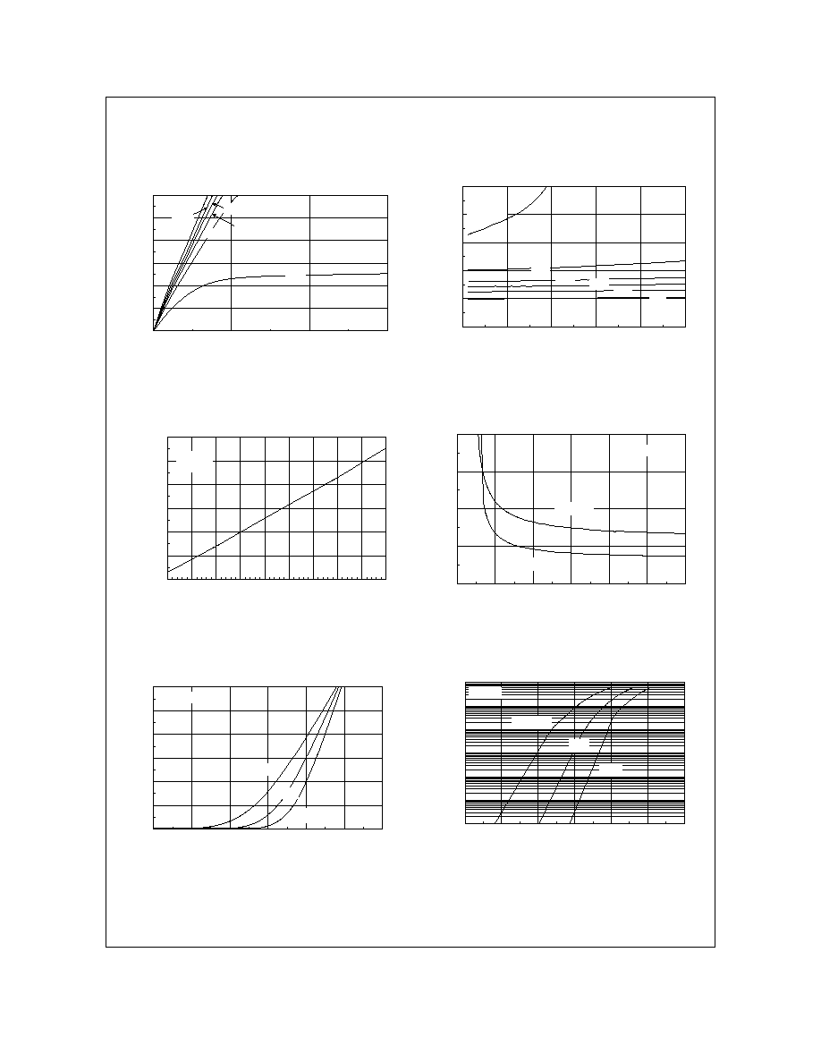
Typical Characteristics
0
10
20
30
40
50
60
0
0.5
1
1.5
V
DS
, DRAIN-SOURCE VOLTAGE (V)
I
D
, DRAIN CURRENT (A)
3.0V
2.0V
2.5V
3.5V
V
GS
= 10V
4.5V
0.5
1
1.5
2
2.5
3
0
10
20
30
40
50
I
D
, DRAIN CURRENT (A)
R
DS
(
O
N)
, NORMALIZED
DRAIN-SOURCE ON-RESISTANCE
V
GS
= 2.0V
3.0V
3.5V
4.5V
2.5V
10V
Figure 1. On-Region Characteristics.
Figure 2. On-Resistance Variation with
Drain Current and Gate Voltage.
0.6
0.8
1
1.2
1.4
1.6
1.8
-50
-25
0
25
50
75
100
125
150
175
T
J
, JUNCTION TEMPERATURE (
o
C)
R
DS
(
O
N)
, NORMALIZED
DRAIN-SOURCE ON-RESISTANCE
I
D
= 16 A
V
GS
= 10V
0.002
0.006
0.01
0.014
0.018
1
2.5
4
5.5
7
8.5
10
V
GS
, GATE TO SOURCE VOLTAGE (V)
R
DS
(
O
N)
, ON-RESISTANCE (OHM)
I
D
= 8 A
T
A
= 125
o
C
T
A
= 25
o
C
Figure 3. On-Resistance Variation
withTemperature.
Figure 4. On-Resistance Variation with
Gate-to-Source Voltage.
0
10
20
30
40
50
60
1
1.25
1.5
1.75
2
2.25
2.5
V
GS
, GATE TO SOURCE VOLTAGE (V)
I
D
, DRAIN CURRENT (A)
T
A
= 125
o
C
25
o
C
-55
o
C
V
DS
= 5V
0.0001
0.001
0.01
0.1
1
10
100
0
0.2
0.4
0.6
0.8
1
1.2
V
SD
, BODY DIODE FORWARD VOLTAGE (V)
I
S
, REVERSE DRAIN CURRENT (A)
T
A
= 125
o
C
25
o
C
-55
o
C
V
GS
= 0V
Figure 5. Transfer Characteristics.
Figure 6. Body Diode Forward Voltage Variation
with Source Current and Temperature.
FDS7064N
FDS7064N Rev C2 (W)
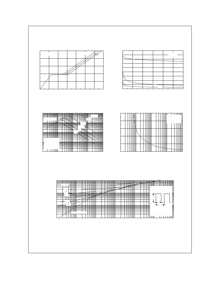
Typical Characteristics
0
1
2
3
4
5
0
5
10
15
20
25
30
35
Q
g
, GATE CHARGE (nC)
V
GS
, GATE-SOURCE VOLTAGE (V)
I
D
= 16 A
V
DS
= 10V
20V
15V
0
500
1000
1500
2000
2500
3000
3500
4000
4500
0
5
10
15
20
25
30
V
DS
, DRAIN TO SOURCE VOLTAGE (V)
CAPACITANCE (pF)
C
ISS
C
RSS
C
OSS
f = 1MHz
V
GS
= 0 V
Figure 7. Gate Charge Characteristics.
Figure 8. Capacitance Characteristics.
0.01
0.1
1
10
100
0.01
0.1
1
10
100
V
DS
, DRAIN-SOURCE VOLTAGE (V)
I
D
, DRAIN CURRENT (A)
DC
1s
100ms
R
DS(ON)
LIMIT
V
GS
= 10V
SINGLE PULSE
R
JA
= 88
o
C/W
T
A
= 25
o
C
10ms
1ms
100µs
0
10
20
30
40
50
0.01
0.1
1
10
100
t
1
, TIME (sec)
P(pk), PEAK TRANSIENT POWER (W)
SINGLE PULSE
R
JA
= 88°C/W
T
A
= 25°C
Figure 9. Maximum Safe Operating Area.
Figure 10. Single Pulse Maximum
Power Dissipation.
0.001
0.01
0.1
1
0.001
0.01
0.1
1
10
100
1000
t
1
, TIME (sec)
r
(t), NORM
AL
IZ
E
D
E
F
F
E
CT
IV
E
T
RANS
IE
NT
T
H
ERM
A
L
RESIST
ANCE
R
JA
(t) = r(t) + R
JA
R
JA
= 85 °C/W
T
J
- T
A
= P * R
JA
(t)
Duty Cycle, D = t
1
/ t
2
P(pk)
t
1
t
2
SINGLE PULSE
0.01
0.02
0.05
0.1
0.2
D = 0.5
Figure 11. Transient Thermal Response Curve.
Thermal characterization performed using the conditions described in Note 1b.
Transient thermal response will change depending on the circuit board design.
FDS7064N
FDS7064N Rev C2 (W)
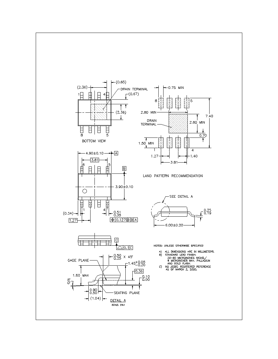
Dimensional Outline and Pad Layout
FDS7064N