©2005 Fairchild Semiconductor Corporation
1
www.fairchildsemi.com
April 2005
FDFM2P110 Rev. C2
FDFM2P110 Integrated P-Channel P
o
werT
renc
h
®
MOSFET and Sc
hottky Diode
FDFM2P110
Integrated P-Channel PowerTrench
®
MOSFET and Schottky Diode
Features
3.5 A, 20 V R
DS(ON)
= 140 m
@ V
GS
= 4.5 V
R
DS(ON)
= 200 m
@ V
GS
= 2.5 V
Low Profile 0.8mm maximum in the new package
MicroFET 3x3 mm
Applications
DC-DC Converter
General Description
FDFM2P110 combines the exceptional performance of Fairchild's
PowerTrench MOSFET technology with a very low forward voltage
drop Schottky barrier rectifier in a MicroFET package.
This device is designed specifically as a single package solution
for DC to DC converters. It features a fast switching, low gate
charge MOSFET with very low on-state resistance.
Absolute Maximum Ratings
T
A
= 25°C unless otherwise noted
Package Marking and Ordering Information
Symbol
Parameter
Ratings
Units
V
DSS
Drain-Source Voltage
20
V
V
GSS
Gate-Source Voltage
±
12
V
I
D
Drain Current
Continuous
(Note 1a)
3.5
A
Pulsed
10
V
RRM
Schottky Repetitive Peak Reverse Voltage
20
V
I
O
Schottky Average Forward Current
(Note 1a)
2
A
P
D
Power Dissipation (Steady State)
(Note 1a)
2.4
W
(Note 1b)
1.2
T
J
, T
STG
Operating and Storage Junction Temperature Range
55 to +150
°
C
Thermal Characteristics
R
JA
Thermal Resistance, Junction-to-Ambient
(Note 1a)
60
°
C/W
R
JA
Thermal Resistance, Junction-to-Ambient
(Note 1b)
145
Device Marking
Device
Reel Size
Tape width
Quantity
2P110
FDFM2P110
7"
12mm 3000
units
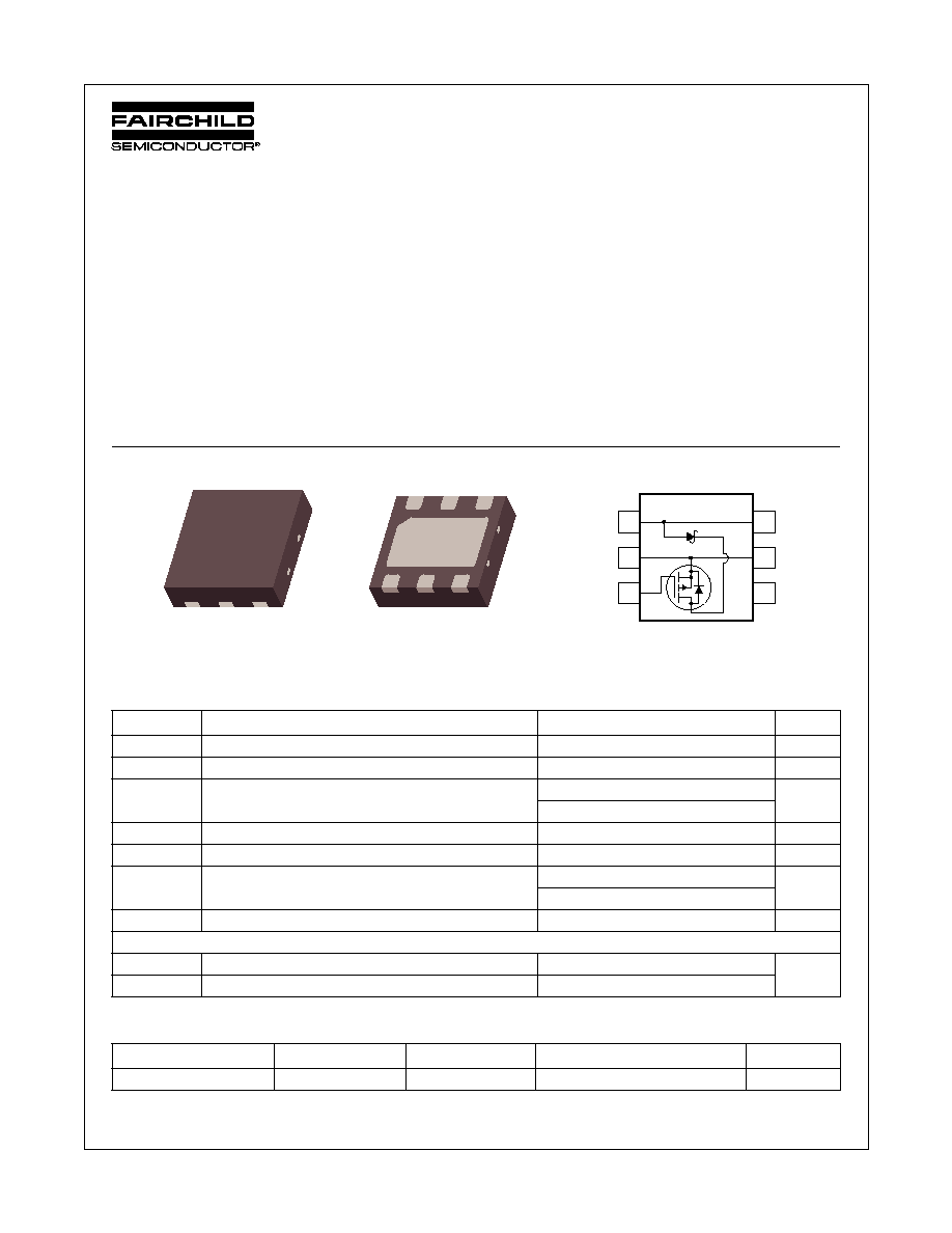
MLP 3x3
Pin 1
Bottom
Top
1
2
3
6
5
4
2
www.fairchildsemi.com
FDFM2P110 Rev. C2
FDFM2P110 Integrated P-Channel P
o
werT
renc
h
®
MOSFET and Sc
hottky Diode
Electrical Characteristics
T
A
= 25°C unless otherwise noted
Symbol
Parameter
Test Conditions
Min
Typ
Max
Units
Off Characteristics
BV
DSS
DrainSource Breakdown Voltage
V
GS
= 0 V, I
D
= 250
µ
A
20
V
BV
DSS
T
J
Breakdown Voltage Temperature
Coefficient
I
D
= 250
µ
A, Referenced to 25
°
C
11
mV/
°
C
I
DSS
Zero Gate Voltage Drain Current
V
DS
= 16 V, V
GS
= 0 V
1
µ
A
I
GSS
GateBody Leakage
V
GS
=
±
12 V, V
DS
= 0 V
±
100
nA
On Characteristics
(Note 2)
V
GS(th)
Gate Threshold Voltage
V
DS
= V
GS
, I
D
= 250
µ
A
0.6
1.0
1.5
V
V
GS(th)
T
J
Gate Threshold Voltage
Temperature Coefficient
I
D
= 250
µ
A, Referenced to 25
°
C
3
mV/
°
C
R
DS(on)
Static DrainSource
OnResistance
V
GS
= 4.5 V, I
D
= 3.5 A
V
GS
= 4.5 V, I
D
= 3.0 A
V
GS
= 4.5 V, I
D
= 3.5A, T
J
= 125
°
C
101
145
136
140
200
202
m
I
D(on)
OnState Drain Current
V
GS
= 2.5 V, V
DS
= 5 V
10
A
g
FS
Forward Transconductance
V
DS
= 5 V, I
D
= 3.5 A
6
S
Dynamic Characteristics
C
iss
Input Capacitance
V
DS
= 10 V, V
GS
= 0 V,
f = 1.0 MHz
280
pF
C
oss
Output Capacitance
65
pF
C
rss
Reverse Transfer Capacitance
35
pF
R
G
Gate Resistance
V
GS
= 0 V, f = 1.0 MHz
7
Switching Characteristics
(Note 2)
t
d(on)
TurnOn Delay Time
V
DD
= 10 V, I
D
= 1 A,
V
GS
= 4.5 V, R
GEN
= 6
8
16
ns
t
r
TurnOn Rise Time
12
22
ns
t
d(off)
TurnOff Delay Time
11
20
ns
t
f
TurnOff Fall Time
3.2
6.4
ns
Q
g
Total Gate Charge
V
DS
= 10 V, I
D
= 3.5 A,
V
GS
= 4.5 V
3
4
nC
Q
gs
GateSource Charge
0.7
nC
Q
gd
GateDrain Charge
1
nC
DrainSource Diode Characteristics and Maximum Ratings
I
S
Maximum Continuous DrainSource Diode Forward Current
2
A
V
SD
DrainSource Diode Forward Voltage V
GS
= 0 V, I
S
= 2 A (Note 2)
0.9
1.2
V
t
rr
Diode Reverse Recovery Time
I
F
= 3.5 A,
dI
F/
dt = 100 A/µs
13
nS
Q
rr
Diode Reverse Recovery Charge
3
nC
Schottky Diode Characteristic
V
R
Reverse Voltage
I
R
= 1 mA
20
V
I
R
Reverse Leakage
V
R
= 5 V
T
J
= 25°C
100
µ
A
T
J
= 100°C
10
mA
V
F
Forward Voltage
I
F
= 1 A
T
J
= 25°C
0.32
0.39
V
3
www.fairchildsemi.com
FDFM2P110 Rev. C2
FDFM2P110 Integrated P-Channel P
o
werT
renc
h
®
MOSFET and Sc
hottky Diode
Notes:
1. R
JA
is the sum of the junction-to-case and case-to-ambient thermal resistance where the case thermal reference is defined as the solder mounting surface of the drain pins.
R
JC
is guaranteed by design while R
CA
is determined by the user's board design.
2. Pulse Test: Pulse Width < 300
µs, Duty Cycle < 2.0%
a) 70°C/W when mounted on
a 1 in
2
pad of 2 oz copper
b) 145°C/W when mounted on a
minimum pad of 2 oz copper
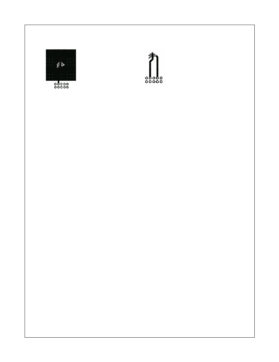
Scale 1 : 1 on letter size paper
4
www.fairchildsemi.com
FDFM2P110 Rev. C2
FDFM2P110 Integrated P-Channel P
o
werT
renc
h
®
MOSFET and Sc
hottky Diode
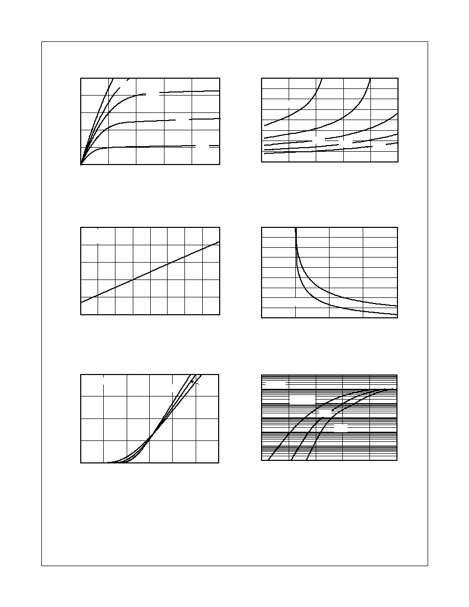
Typical Characteristics
0
2
4
6
8
10
0
1
2
3
4
5
-V
DS
, DRAIN-SOURCE VOLTAGE (V)
-I
D
, DRAIN CURRENT (A)
-2.5V
-2.0V
V
GS
= -4.5V
-3.0V
-3.5V
0.8
1
1.2
1.4
1.6
1.8
2
2.2
2.4
0
2
4
6
8
10
-I
D
, DRAIN CURRENT (A)
R
DS(ON)
, NORMALIZED
DRAIN-SOURCE ON-RESISTANCE
V
GS
= -2.5V
-4.0V
-3.5V
-4.5V
-3.0V
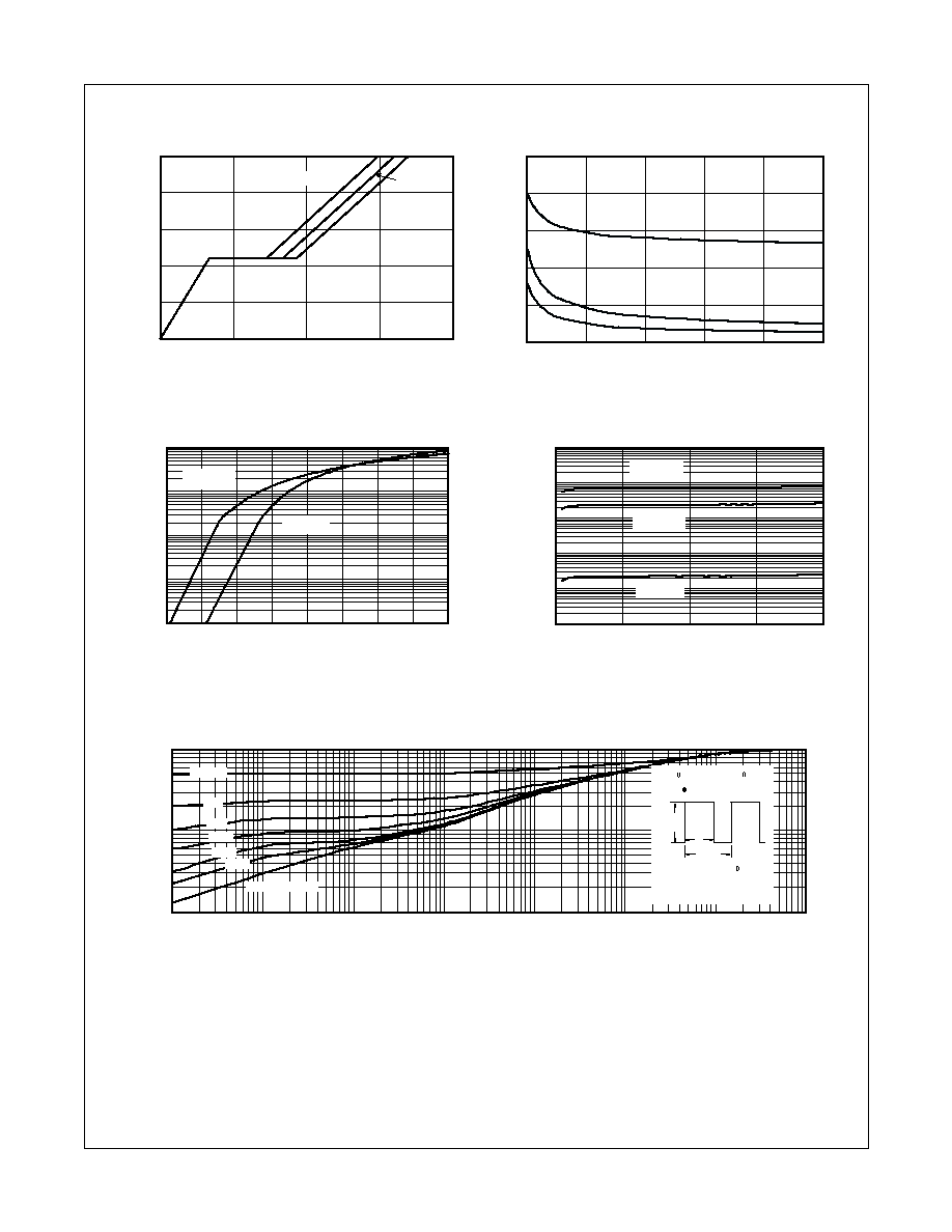
Figure 1. On-Region Characteristics.
Figure 2. On-Resistance Variation with
Drain Current and Gate Voltage.
0.6
0.8
1
1.2
1.4
1.6
-50
-25
0
25
50
75
100
125
150
T
J
, JUNCTION TEMPERATURE (
°C)
R
DS(ON)
, NORMALIZED
DRAIN-SOURCE ON-RESISTANCE
I
D
= -3.5A
V
GS
= -4.5V
0.08
0.12
0.16
0.2
0.24
0.28
0.32
0.36
0.4
0.44
1
2
3
4
5
-V
GS
, GATE TO SOURCE VOLTAGE (V)
R
DS(ON)
, ON-RESISTANCE (OHM)
I
D
= -1.8A
T
A
= 125
°C
T
A
= 25
°C
Figure 3. On-Resistance Variation with
Temperature.
Figure 4. On-Resistance Variation with
Gate-to-Source Voltage.
0
2
4
6
8
0.5
1
1.5
2
2.5
3
3.5
-V
GS
, GATE TO SOURCE VOLTAGE (V)
-I
D
, DRAIN CURRENT (A)
T
A
= -55
°C
25
°C
125
°C
V
DS
= -5V
0.0001
0.001
0.01
0.1
1
10
100
0.2
0.4
0.6
0.8
1
1.2
-V
SD
, BODY DIODE FORWARD VOLTAGE (V)
-I
S
, REVERSE DRAIN CURRENT (A)
T
A
= 125
°C
25
°C
-55
°C
V
GS
= 0V
Figure 5. Transfer Characteristics.
Figure 6. Body Diode Forward Voltage Variation
with Source Current and Temperature.
5
www.fairchildsemi.com
FDFM2P110 Rev. C2
FDFM2P110 Integrated P-Channel P
o
werT
renc
h
®
MOSFET and Sc
hottky Diode
Typical Characteristics
0
1
2
3
4
5
0
1
2
3
4
Q
g
, GATE CHARGE (nC)
-V
GS
, GATE-SOURCE VOLTAGE (V)
I
D
= -3.5A
V
DS
= -5V
-15V
-10V
0
100
200
300
400
500
0
4
8
12
16
20
-V
DS
, DRAIN TO SOURCE VOLTAGE (V)
CAPACITANCE (pF)
C
iss
C
rss
C
oss
f = 1MHz
V
GS
= 0 V
Figure 7. Gate Charge Characteristics.
Figure 8. Capacitance Characteristics.
0.001
0.01
0.1
1
10
0
0.1
0.2
0.3
0.4
0.5
0.6
0.7
0.8
V
F
, FORWARD VOLTAGE (V)
I
F
, FORWARD LEAKAGE CURRENT (A)
T
J
= 25
°C
T
J
= 125
°C
0.000001
0.00001
0.0001
0.001
0.01
0.1
0
5
10
15
20
V
R
, REVERSE VOLTAGE (V)
I
R
, REVERSE LEAKAGE CURRENT (A)
T
J
= 25
°C
T
J
= 125
°C
T
J
= 100
°C
Figure 9. Schottky Diode Forward Voltage.
Figure 10. Schottky Diode Reverse Current.
0.01
0.1
1
0.0001
0.001
0.01
0.1
1
10
100
1000
t
1
, TIME (sec)
r(t), NORMALIZED EFFECTIVE TRANSIENT
THERMAL RESISTANCE
R
JA
(t) = r(t) * R
JA
R
JA
=145
°C/W
T
J
- T
A
= P * R
JA
(t)
Duty Cycle, D = t
1
/ t
2
P(pk)
t
1
t
2
SINGLE PULSE
0.01
0.02
0.05
0.1
0.2
D = 0.5
Figure 11. Transient Thermal Response Curve.
Thermal characterization performed using the conditions described in Note 1b.
Transient thermal response will change depending on the circuit board design.
6
www.fairchildsemi.com
FDFM2P110 Rev. C2
FDFM2P110 Integrated P-Channel P
o
werT
renc
h
®
MOSFET and Sc
hottky Diode
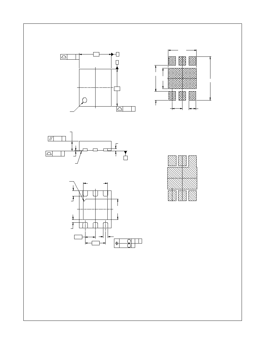
Package Dimensions
B. DIMENSIONS ARE IN MILLIMETERS.
C. DIMENSIONS AND TOLERANCES PER ASME Y14.5M, 1994
NOTES:
A. CONFORMS TO JEDEC REGISTRATION MO-229,
VARIATION WEEA, DATED 11/2001
2X
2X
TOP VIEW
SIDE VIEW
BOTTOM VIEW
RECOMMENDED LAND PATTERN
RECOMMENDED COPPER TRACE
0.15
0.15
0.10
(0.20)
1.65
MAX
0.2 MIN
0.95
1.90
0.30~0.45
0.10
C
C
A B
0.05
M
M
0.8 MAX
0.05
0.00
0.45
0.20
SEATING
PLANE
0.08
C
C
C
2.25 MAX
PIN #1 IDENT
C
C
3.0
3.0
2.65
2.10
(0.70)
0.95 TYP
0.65 TYP
1.65
3.50
6
4
6
6
4
4
1
1
1
3
3
3
A
B
PIN #1 IDENT

7
www.fairchildsemi.com
FDFM2P110 Rev. C2
FDFM2P110 Integrated P-Channel P
o
werT
renc
h
®
MOSFET and Sc
hottky Diode
DISCLAIMER
FAIRCHILD SEMICONDUCTOR RESERVES THE RIGHT TO MAKE CHANGES WITHOUT FURTHER NOTICE TO ANY
PRODUCTS HEREIN TO IMPROVE RELIABILITY, FUNCTION OR DESIGN. FAIRCHILD DOES NOT ASSUME ANY LIABILITY
ARISING OUT OF THE APPLICATION OR USE OF ANY PRODUCT OR CIRCUIT DESCRIBED HEREIN; NEITHER DOES IT
CONVEY ANY LICENSE UNDER ITS PATENT RIGHTS, NOR THE RIGHTS OF OTHERS.
TRADEMARKS
The following are registered and unregistered trademarks Fairchild Semiconductor owns or is authorized to use and is
not intended to be an exhaustive list of all such trademarks.
LIFE SUPPORT POLICY
FAIRCHILD'S PRODUCTS ARE NOT AUTHORIZED FOR USE AS CRITICAL COMPONENTS IN LIFE SUPPORT
DEVICES OR SYSTEMS WITHOUT THE EXPRESS WRITTEN APPROVAL OF FAIRCHILD SEMICONDUCTOR CORPORATION.
As used herein:
1. Life support devices or systems are devices or
systems which, (a) are intended for surgical implant into
the body, or (b) support or sustain life, or (c) whose
failure to perform when properly used in accordance
with instructions for use provided in the labeling, can be
reasonably expected to result in significant injury to the
user.
2. A critical component is any component of a life
support device or system whose failure to perform can
be reasonably expected to cause the failure of the life
support device or system, or to affect its safety or
effectiveness.
PRODUCT STATUS DEFINITIONS
Definition of Terms
Datasheet Identification
Product Status
Definition
Advance Information
Preliminary
No Identification Needed
Obsolete
This datasheet contains the design specifications for
product development. Specifications may change in
any manner without notice.
This datasheet contains preliminary data, and
supplementary data will be published at a later date.
Fairchild Semiconductor reserves the right to make
changes at any time without notice in order to improve
design.
This datasheet contains final specifications. Fairchild
Semiconductor reserves the right to make changes at
any time without notice in order to improve design.
This datasheet contains specifications on a product
that has been discontinued by Fairchild semiconductor.
The datasheet is printed for reference information only.
Formative or
In Design
First Production
Full Production
Not In Production
IntelliMAXTM
ISOPLANARTM
LittleFETTM
MICROCOUPLERTM
MicroFETTM
MicroPakTM
MICROWIRETM
MSXTM
MSXProTM
OCXTM
OCXProTM
OPTOLOGIC
OPTOPLANARTM
PACMANTM
FAST
FASTrTM
FPSTM
FRFETTM
GlobalOptoisolatorTM
GTOTM
HiSeCTM
I
2
CTM
i-LoTM
ImpliedDisconnectTM
Rev. I15
ACExTM
ActiveArrayTM
BottomlessTM
CoolFETTM
CROSSVOLTTM
DOMETM
EcoSPARKTM
E
2
CMOSTM
EnSignaTM
FACTTM
FACT Quiet SeriesTM
POPTM
Power247TM
PowerEdgeTM
PowerSaverTM
PowerTrench
QFET
QSTM
QT OptoelectronicsTM
Quiet SeriesTM
RapidConfigureTM
RapidConnectTM
µSerDesTM
SILENT SWITCHER
SMART STARTTM
SPMTM
StealthTM
SuperFETTM
SuperSOTTM-3
SuperSOTTM-6
SuperSOTTM-8
SyncFETTM
TinyLogic
TINYOPTOTM
TruTranslationTM
UHCTM
UltraFET
UniFETTM
VCXTM
Across the board. Around the world.TM
The Power Franchise
Programmable Active DroopTM