
June 2004
2004 Fairchild Semiconductor Corporation
FDC6000NZ Rev E1 (W)
FDC6000NZ
Dual N-Channel 2.5V Specified PowerTrench
MOSFET
General Description
This N-Channel 2.5V specified MOSFET is a rugged
gate version of Fairchild's Semiconductor's advanced
PowerTrench process. It has been optimized for power
management applications with a wide range of gate
drive voltage (2.5V 12V). Packaged in FLMP SSOT-6,
the R
DS(ON)
and thermal properties of the device are
optimized for battery power management applications.
Applications
· Battery management/Charger Application
· Load switch
Features
· 6.5 A, 20 V R
DS(ON)
= 20 m
@ V
GS
= 4.5 V
R
DS(ON)
= 28 m
@ V
GS
= 2.5 V
· ESD protection diode (note 3)
· High performance trench technology for extremely
low R
DS(ON)
· FLMP SSOT-6 package: Enhanced thermal
performance in industry-standard package size
3
2
1
4
5
6
Bottom Drain Contact
Bottom Drain Contact
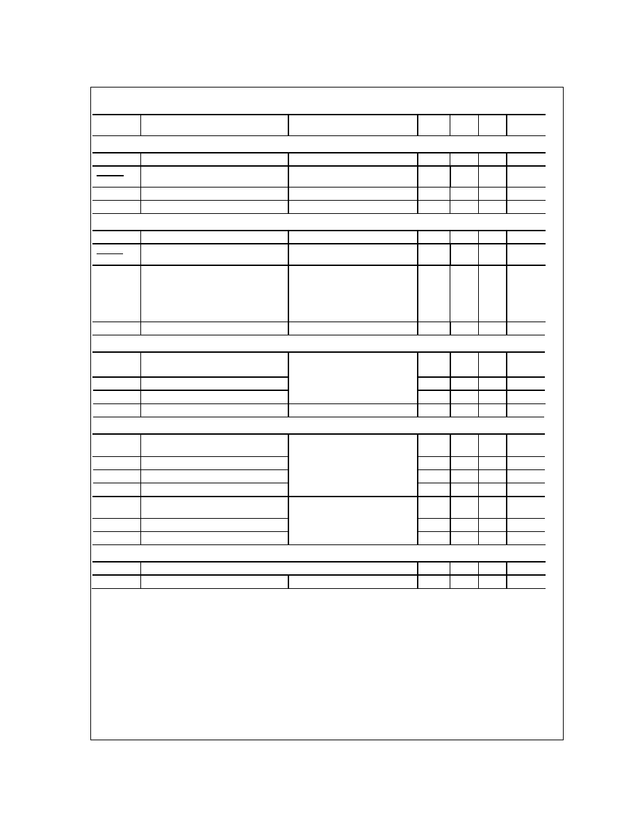
MOSFET Maximum Ratings
T
A
=25
o
C unless otherwise noted
Symbol Parameter
Ratings
Units
V
DSS
Drain-Source Voltage
20
V
V
GSS
Gate-Source
Voltage
±12
V
I
D
Drain Current Continuous
(Note 1a)
7.3 A
Pulsed
20
P
D
Power Dissipation for Dual Operation
(Note 1a)
1.6 W
Power Dissipation for Single Operation
(Note 1a)
1.8
(Note 1b)
1.2
T
J
, T
STG
Operating and Storage Junction Temperature Range
55 to +150
°C
Thermal Characteristics
R
JA
Thermal Resistance, Junction-to-Ambient
(Note 1a)
68
°C/W
R
Jc
Thermal Resistance, Junction-to-Case
(Note 1a)
1
Package Marking and Ordering Information
Device Marking
Device
Reel Size
Tape width
Quantity
.0NZ FDC6000NZ
7''
8mm
3000
units
FDC6000NZ
SuperSOT-6
TM
FLMP
G1
S1
S1
S2
G2
S2
SuperSOT-6
TM
FLMP
G1
S1
S1
S2
G2
S2
FDC6000NZ RevE1 (W)
Electrical Characteristics
T
A
= 25°C unless otherwise noted
Symbol Parameter
Test
Conditions
Min
Typ
Max
Units
Off Characteristics
BV
DSS
DrainSource Breakdown Voltage
V
GS
= 0 V,
I
D
= 250
µA
20 V
BV
DSS
T
J
Breakdown Voltage Temperature
Coefficient
I
D
= 250
µA, Referenced to 25°C
14
mV/
°C
I
DSS
Zero Gate Voltage Drain Current
V
DS
= 16 V,
V
GS
= 0 V
1
µA
I
GSS
GateBody
Leakage
V
GS
=
±12 V,
V
DS
= 0 V
± 10
µA
On Characteristics
(Note 2)
V
GS(th)
Gate Threshold Voltage
V
DS
= V
GS
,
I
D
= 250
µA
0.6 0.9 1.5 V
V
GS(th)
T
J
Gate Threshold Voltage
Temperature Coefficient
I
D
= 250
µA, Referenced to 25°C
4
mV/
°C
R
DS(on)
Static DrainSource
OnResistance
V
GS
= 4.5 V,
I
D
= 6.5 A
V
GS
= 4.0 V,
I
D
= 6.4 A
V
GS
= 3.1 V,
I
D
= 6.3 A
V
GS
= 2.5 V,
I
D
= 5.5 A
V
GS
= 4.5 V, I
D
= 6.5A, T
J
=125
°C
16.5
16.8
19.2
22.5
22.8
20
21
24
28
30
m
g
FS
Forward
Transconductance
V
DS
= 5 V,
I
D
= 6.5 A
30
S
Dynamic Characteristics
C
iss
Input
Capacitance
V
DS
= 10 V,
V
GS
= 0 V,
f = 1.0 MHz
840 pF
C
oss
Output
Capacitance
210
pF
C
rss
Reverse Transfer Capacitance
100 pF
R
G
Gate
Resistance
V
GS
= 15 mV, f = 1.0 MHz
2.3
Switching Characteristics
(Note 2)
t
d(on)
TurnOn
Delay
Time
V
DD
= 10 V,
I
D
= 1 A,
V
GS
= 4.5 V,
R
GEN
= 6
10
20 ns
t
r
TurnOn Rise Time
15
27
ns
t
d(off)
TurnOff Delay Time
18
32
ns
t
f
TurnOff
Fall
Time
9
18 ns
Q
g
Total Gate Charge
V
DS
= 10 V,
I
D
= 6.5 A,
V
GS
= 4.5 V
8
11
nC
Q
gs
GateSource
Charge
1.5
nC
Q
gd
GateDrain
Charge
2.1 nC
DrainSource Diode Characteristics and Maximum Ratings
I
S
Maximum Continuous DrainSource Diode Forward Current
1.25
A
V
SD
DrainSource Diode Forward Voltage V
GS
= 0 V, I
S
= 1.25A
(Note 2)
0.7
1.2 V
FDC6000NZ
FDC6000NZ RevE1 (W)
Electrical Characteristics
T
A
= 25°C unless otherwise noted
Symbol Parameter
Test
Conditions
Min
Typ
Max
Units
DrainSource Diode Characteristics and Maximum Ratings
t
rr
Diode Reverse Recovery Time
I
F
= 6.5 A, d
iF
/d
t
= 100 A/µs
16 nS
Q
rr
Diode Reverse Recovery Charge
4.3
nC
NOTES:
1. R
JA
is the sum of the junction-to-case and case-to-ambient thermal resistance where the case thermal reference is defined as the solder mounting surface of
the
drain pins. R
JC
is guaranteed by design while R
CA
is determined by the user's board design.
a) 68°C/W
when
mounted on a 1in
2
pad
of 2 oz copper (Single
Operation).
b) 102°C/W
when
mounted
on a minimum pad of 2 oz
copper (Single Operation).
Scale 1 : 1 on letter size paper
2. Pulse Test: Pulse Width < 300
µs, Duty Cycle < 2.0%
3. The diode connected between the gate and source serves only as protection against ESD. No gate overvoltage rating is implied.
4. Electrical characterization and datasheet limits was based on a single source configuration (pin 2 & 5 no connection).
FDC6000NZ

FDC6000NZ RevE1 (W)
Dimensional Outline and Pad Layout
Bottom View
Top View
Recommended Landing Pattern
For Common Drain Configuration
Recommended Landing Pattern
For Standard Dual Configuration
FDC6000NZ

FDC6000NZ Rev E1(W)
Typical Characteristics
0
5
10
15
20
0
0.5
1
1.5
2
2.5
V
DS
, DRAIN-SOURCE VOLTAGE (V)
I
D
,
DRAI
N CURRENT (
A
)
1.8V
3.5V
V
GS
= 4.5V
2.5V
2.0V
3.0V
0.8
1
1.2
1.4
1.6
1.8
2
2.2
2.4
2.6
2.8
3
0
5
10
15
20
I
D
, DRAIN CURRENT (A)
R
DS(O
N)
,
NORMALI
Z
ED
DRAI
N-
SOURCE ON-
R
ESI
STANCE
V
GS
= 1.8V
3.5V
4.5V
3.0V
2.5V
2.0V
Figure 1. On-Region Characteristics.
Figure 2. On-Resistance Variation with
Drain Current and Gate Voltage.
0.6
0.8
1
1.2
1.4
1.6
-50
-25
0
25
50
75
100
125
150
T
J
, JUNCTION TEMPERATURE (
o
C)
R
DS
(
O
N)
, NORMALIZED
DRAIN-SOURCE ON-RESISTANCE
I
D
= 6.5A
V
GS
= 4.5V
0.012
0.017
0.022
0.027
0.032
0.037
0.042
0.047
0.052
0.057
0.062
1
2
3
4
5
V
GS
, GATE TO SOURCE VOLTAGE (V)
R
DS
(
O
N)
, ON-
R
E
S
I
S
T
ANCE
(
O
HM)
I
D
= 3.3 A
T
A
= 125
o
C
T
A
= 25
o
C
Figure 3. On-Resistance Variation with
Temperature.
Figure 4. On-Resistance Variation with
Gate-to-Source Voltage.
0
5
10
15
20
25
30
1
1.5
2
2.5
V
GS
, GATE TO SOURCE VOLTAGE (V)
I
D
, DRAIN CURRENT (A)
T
A
= -55
o
C
25
o
C
125
o
C
V
DS
= 5V
0.0001
0.001
0.01
0.1
1
10
100
0
0.2
0.4
0.6
0.8
1
1.2
V
SD
, BODY DIODE FORWARD VOLTAGE (V)
I
S
, REVERSE DRAIN CURRENT (A)
T
A
= 125
o
C
25
o
C
-55
o
C
V
GS
= 0V
Figure 5. Transfer Characteristics.
Figure 6. Body Diode Forward Voltage Variation
with Source Current and Temperature.
FDC6000NZ