©2004 Fairchild Semiconductor Corporation
November 2004
FDB8874 Rev. A2
FDB8874
FDB8874
N-Channel PowerTrench
®
MOSFET
30V, 121A, 4.7m
General Description
This N-Channel MOSFET has been designed specifically to
improve the overall efficiency of DC/DC converters using
either synchronous or conventional switching PWM
controllers. It has been optimized for low gate charge, low
r
DS(ON)
and fast switching speed.
Applications
· DC/DC converters
Features
· r
DS(ON)
= 4.7m
, V
GS
= 10V, I
D
= 40A
· r
DS(ON)
= 6.0m
, V
GS
= 4.5V, I
D
= 40A
· High performance trench technology for extremely low
r
DS(ON)
· Low gate charge
· High power and current handling capability
MOSFET Maximum Ratings
T
C
= 25°C unless otherwise noted
Thermal Characteristics
Package Marking and Ordering Information
Symbol
Parameter
Ratings
Units
V
DSS
Drain to Source Voltage
30
V
V
GS
Gate to Source Voltage
±
20
V
I
D
Drain Current
121
A
Continuous (T
C
= 25
o
C, V
GS
= 10V) (Note 1)
Continuous (T
C
= 25
o
C, V
GS
= 4.5V) (Note 1)
107
A
Continuous (T
amb
= 25
o
C, V
GS
= 10V, with R
JA
= 43
o
C/W)
21
A
Pulsed
Figure 4
A
E
AS
Single Pulse Avalanche Energy (Note 2)
105
mJ
P
D
Power dissipation
110
W
Derate above 25
o
C
0.73
W/
o
C
T
J
, T
STG
Operating and Storage Temperature
-55 to 175
o
C
R
JC
Thermal Resistance Junction to Case TO-263
1.36
o
C/W
R
JA
Thermal Resistance Junction to Ambient TO-263 ( Note 3)
62
o
C/W
R
JA
Thermal Resistance Junction to Ambient TO-263, 1in
2
copper pad area
43
o
C/W
Device Marking
Device
Package
Reel Size
Tape Width
Quantity
FDB8874
FDB8874
TO-263AB
330mm
24mm
800 units
FDB8874
FDB8874_NL (Note 4)
TO-263AB
330mm
24mm
800 units
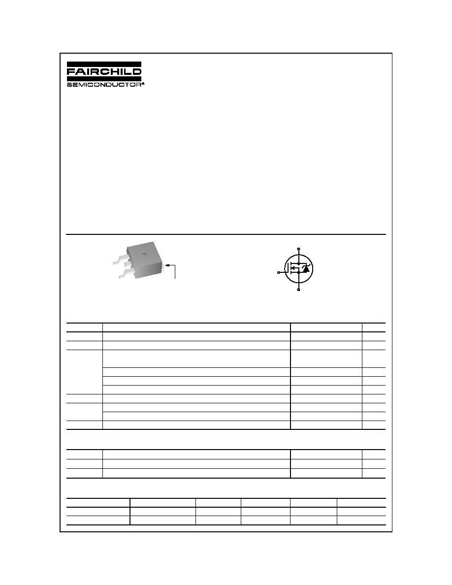
D
G
S
TO-263AB
FDB SERIES
GATE
SOURCE
DRAIN
(FLANGE)

©2004 Fairchild Semiconductor Corporation
FDB8874 Rev. A2
FDB8874
Electrical Characteristics
T
C
= 25°C unless otherwise noted
Off Characteristics
On Characteristics
Dynamic Characteristics
Switching Characteristics
(V
GS
= 10V)
Drain-Source Diode Characteristics
Notes:
1: Package current limitation is 80A.
2: Starting T
J
= 25°C, L = 51uH, I
AS
= 64A, V
DD
= 27V, V
GS
= 10V.
3: Pulse width = 100s.
4: FDB8874_NL is lead free product. FDB8874_NL marking will appear on the reel label.
Symbol
Parameter
Test Conditions
Min
Typ
Max
Units
B
VDSS
Drain to Source Breakdown Voltage
I
D
= 250
µ
A, V
GS
= 0V
30
-
-
V
I
DSS
Zero Gate Voltage Drain Current
V
DS
= 24V
-
-
1
µ
A
V
GS
= 0V
T
C
= 150
o
C
-
-
250
I
GSS
Gate to Source Leakage Current
V
GS
=
±
20V
-
-
±
100
nA
V
GS(TH)
Gate to Source Threshold Voltage
V
GS
= V
DS
, I
D
= 250
µ
A
1.2
-
2.5
V
r
DS(ON)
Drain to Source On Resistance
I
D
= 40A, V
GS
= 10V
-
0.0033 0.0047
I
D
= 40A, V
GS
= 4.5V
-
0.0041 0.0060
I
D
= 40A, V
GS
= 10V,
T
J
= 175
o
C
-
0.0062 0.0080
C
ISS
Input Capacitance
V
DS
= 15V, V
GS
= 0V,
f = 1MHz
-
3130
-
pF
C
OSS
Output Capacitance
-
590
-
pF
C
RSS
Reverse Transfer Capacitance
-
345
-
pF
R
G
Gate Resistance
V
GS
= 0.5V, f = 1MHz
-
1.9
-
Q
g(TOT)
Total Gate Charge at 10V
V
GS
= 0V to 10V
V
DD
= 15V
I
D
= 40A
I
g
= 1.0mA
-
56
72
nC
Q
g(5)
Total Gate Charge at 5V
V
GS
= 0V to 5V
-
30
38
nC
Q
g(TH)
Threshold Gate Charge
V
GS
= 0V to 1V
-
3.0
4.0
nC
Q
gs
Gate to Source Gate Charge
-
9.0
-
nC
Q
gs2
Gate Charge Threshold to Plateau
-
6.0
-
nC
Q
gd
Gate to Drain "Miller" Charge
-
11
-
nC
t
ON
Turn-On Time
V
DD
= 15V, I
D
= 40A
V
GS
= 10V, R
GS
= 4.7
-
-
217
ns
t
d(ON)
Turn-On Delay Time
-
10
-
ns
t
r
Rise Time
-
135
-
ns
t
d(OFF)
Turn-Off Delay Time
-
45
-
ns
t
f
Fall Time
-
34
-
ns
t
OFF
Turn-Off Time
-
-
118
ns
V
SD
Source to Drain Diode Voltage
I
SD
= 40A
-
-
1.25
V
I
SD
= 20A
-
-
1.0
V
t
rr
Reverse Recovery Time
I
SD
= 40A, dI
SD
/dt = 100A/
µ
s
-
-
32
ns
Q
RR
Reverse Recovered Charge
I
SD
= 40A, dI
SD
/dt = 100A/
µ
s
-
-
18
nC
©2004 Fairchild Semiconductor Corporation
FDB8874 Rev. A2
FDB8874
Typical Characteristics
T
C
= 25°C unless otherwise noted
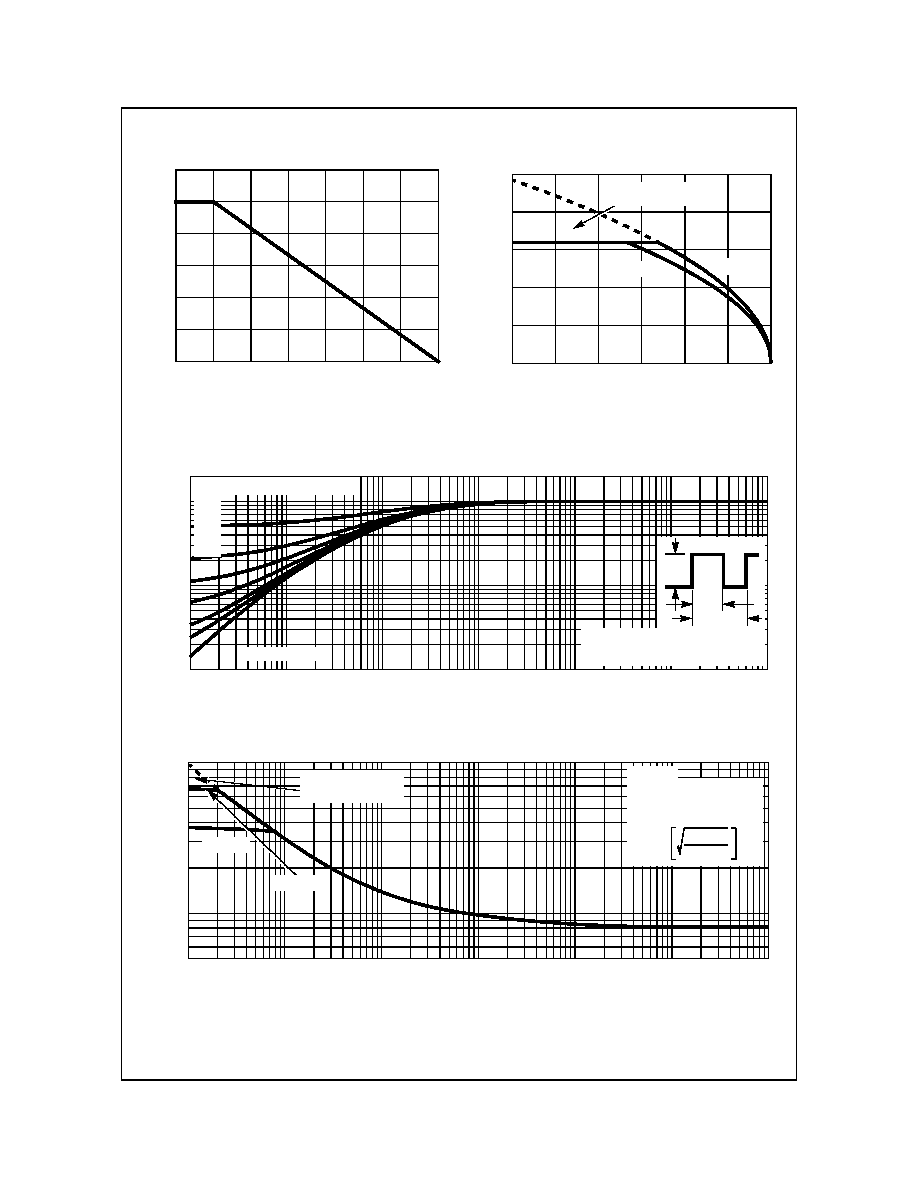
Figure 1. Normalized Power Dissipation vs Case
Temperature
Figure 2. Maximum Continuous Drain Current vs
Case Temperature
Figure 3. Normalized Maximum Transient Thermal Impedance
Figure 4. Peak Current Capability
T
C
, CASE TEMPERATURE (
o
C)
P
O
W
E
R DIS
S
I
P
A
T
ION M
U
L
T
IP
L
I
E
R
0
0
25
50
75
100
175
0.2
0.4
0.6
0.8
1.0
1.2
125
150
0
25
50
75
100
125
25
50
75
100
125
150
175
I
D
, DRAIN CURRENT
(
A
)
T
C
, CASE TEMPERATURE (
o
C)
V
GS
= 10V
V
GS
= 4.5V
CURRENT LIMITED
BY PACKAGE
0.1
1
10
-5
10
-4
10
-3
10
-2
10
-1
10
0
10
1
0.01
2
t, RECTANGULAR PULSE DURATION (s)
Z
JC
, NORM
AL
IZ
ED
TH
ERM
A
L I
M
PED
AN
CE
NOTES:
DUTY FACTOR: D = t
1
/t
2
PEAK T
J
= P
DM
x Z
JC
x R
JC
+ T
C
P
DM
t
1
t
2
0.5
0.2
0.1
0.05
0.01
0.02
DUTY CYCLE - DESCENDING ORDER
SINGLE PULSE
100
1000
50
I
DM
,
P
E
AK CURRE
NT
(
A
)
t, PULSE WIDTH (s)
10
-5
10
-4
10
-3
10
-2
10
-1
10
0
10
1
T
C
= 25
o
C
I = I
25
175 - T
C
150
FOR TEMPERATURES
ABOVE 25
o
C DERATE PEAK
CURRENT AS FOLLOWS:
TRANSCONDUCTANCE
MAY LIMIT CURRENT
IN THIS REGION
V
GS
= 4.5V
V
GS
= 10V
©2004 Fairchild Semiconductor Corporation
FDB8874 Rev. A2
FDB8874
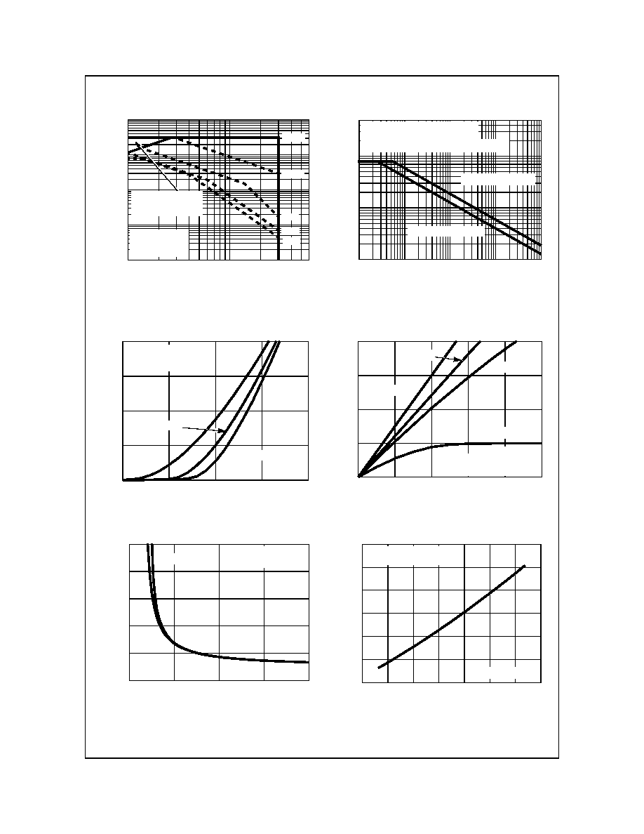
Figure 5. Forward Bias Safe Operating Area
NOTE: Refer to Fairchild Application Notes AN7514 and AN7515
Figure 6. Unclamped Inductive Switching
Capability
Figure 7. Transfer Characteristics
Figure 8. Saturation Characteristics
Figure 9. Drain to Source On Resistance vs Gate
Voltage and Drain Current
Figure 10. Normalized Drain to Source On
Resistance vs Junction Temperature
Typical Characteristics
T
C
= 25°C unless otherwise noted
0.1
1
10
100
1000
1
10
60
V
DS
, DRAIN TO SOURCE VOLTAGE (V)
I
D
,
DR
AIN
C
URRENT
(
A
)
T
J
= MAX RATED
T
C
= 25
o
C
SINGLE PULSE
LIMITED BY r
DS(ON)
AREA MAY BE
OPERATION IN THIS
10
µ
s
1ms
DC
100
µ
s
10ms
1
10
100
0.01
0.1
1
10
500
100
I
AS
, A
V
AL
ANCHE CURR
ENT
(
A
)
t
AV
, TIME IN AVALANCHE (ms)
STARTING T
J
= 25
o
C
STARTING T
J
= 150
o
C
t
AV
= (L)(I
AS
)/(1.3*RATED BV
DSS
- V
DD
)
If R = 0
If R
0
t
AV
= (L/R)ln[(I
AS
*R)/(1.3*RATED BV
DSS
- V
DD
) +1]
0
40
80
120
160
2.0
2.5
3.0
3.5
4.0
I
D
, DRAIN CURR
ENT
(
A
)
V
GS
, GATE TO SOURCE VOLTAGE (V)
PULSE DURATION = 80
µ
s
DUTY CYCLE = 0.5% MAX
V
DD
= 15V
T
J
= 175
o
C
T
J
= -55
o
C
T
J
= 25
o
C
0
40
80
120
160
0
0.2
0.4
0.6
0.8
1.0
I
D
,
DRA
I
N
C
URRENT
(
A
)
V
DS
, DRAIN TO SOURCE VOLTAGE (V)
PULSE DURATION = 80
µ
s
DUTY CYCLE = 0.5% MAX
T
C
= 25
o
C
V
GS
= 10V
V
GS
= 4V
V
GS
= 3V
V
GS
= 5V
2
4
6
8
10
12
2
4
6
8
10
I
D
= 1A
V
GS
, GATE TO SOURCE VOLTAGE (V)
I
D
= 40A
r
DS(
O
N)
, DRAIN T
O
S
O
U
RCE
ON RES
I
ST
ANCE
(
m
)
PULSE DURATION = 80
µ
s
DUTY CYCLE = 0.5% MAX
0.6
0.8
1.0
1.2
1.4
1.6
1.8
-80
-40
0
40
80
120
160
200
NORM
AL
IZ
ED DRAIN T
O
S
O
URCE
T
J
, JUNCTION TEMPERATURE (
o
C)
ON RES
I
ST
ANCE
V
GS
= 10V, I
D
= 40A
PULSE DURATION = 80
µ
s
DUTY CYCLE = 0.5% MAX
©2004 Fairchild Semiconductor Corporation
FDB8874 Rev. A2
FDB8874
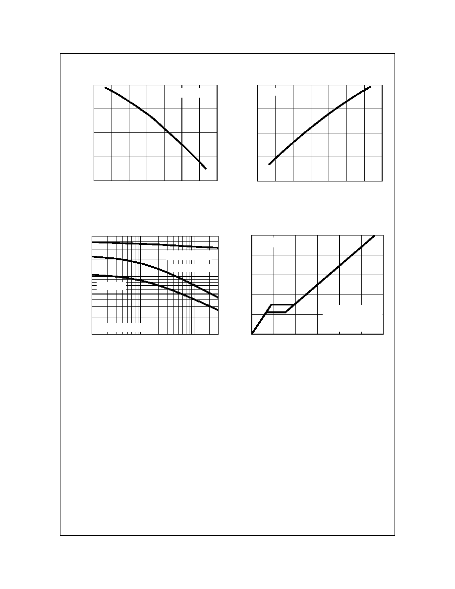
Figure 11. Normalized Gate Threshold Voltage vs
Junction Temperature
Figure 12. Normalized Drain to Source
Breakdown Voltage vs Junction Temperature
Figure 13. Capacitance vs Drain to Source
Voltage
Figure 14. Gate Charge Waveforms for Constant
Gate Current
Typical Characteristics
T
C
= 25°C unless otherwise noted
0.4
0.6
0.8
1.0
1.2
-80
-40
0
40
80
120
160
200
V
GS
= V
DS
, I
D
= 250
µ
A
NORM
AL
IZ
E
D
GA
T
E
T
J
, JUNCTION TEMPERATURE (
o
C)
T
HRE
SHOL
D V
O
L
T
A
GE
0.90
0.95
1.00
1.05
1.10
-80
-40
0
40
80
120
160
200
T
J
, JUNCTION TEMPERATURE (
o
C)
NORM
AL
IZ
ED DRAIN T
O
S
O
URCE
I
D
= 250
µ
A
BRE
AKDO
WN V
O
L
T
A
GE
100
1000
0.1
1
10
30
5000
C, CA
P
A
CIT
ANCE
(
p
F
)
V
DS
, DRAIN TO SOURCE VOLTAGE (V)
V
GS
= 0V, f = 1MHz
C
ISS
=
C
GS
+ C
GD
C
OSS
C
DS
+ C
GD
C
RSS
=
C
GD
0
2
4
6
8
10
0
10
20
30
40
50
60
V
GS
,
GA
T
E
T
O
SOURCE
V
O
L
T
A
GE (
V
)
Q
g
, GATE CHARGE (nC)
V
DD
= 15V
I
D
= 40A
I
D
= 1A
WAVEFORMS IN
DESCENDING ORDER: