January 2006
FDB8860 N-Channel Logi
c Level
P
o
werTrench
®
MO
SFE
T
©2005 Fairchild Semiconductor Corporation
FDB8860 Rev A
www.fairchildsemi.com
1
FDB8860
N-Channel Logic Level
PowerTrench
®
MOSFET
30V, 80A, 2.6m
Features
R
DS(ON)
= 1.9m
(Typ), V
GS
= 5V, I
D
= 80A
Q
g(5)
= 89nC (Typ), V
GS
= 5V
Low Miller Charge
Low Q
RR
Body Diode
UIS Capability (Single Pulse and Repetitive Pulse)
Qualified to AEC Q101
RoHS Compliant
Applications
12V Automotive Load Control
Start / Alternator Systems
Electronic Power Steering Systems
ABS
DC-DC Converters
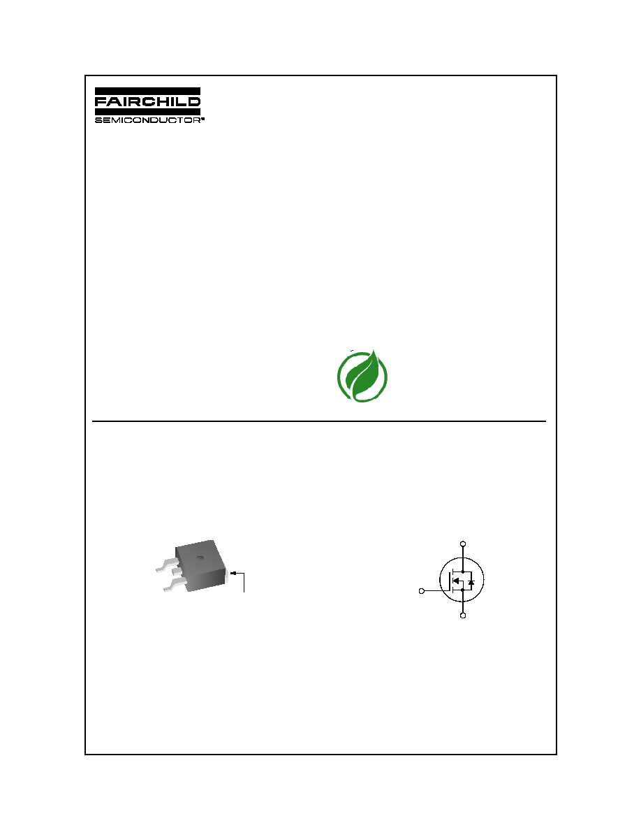
D
G
S
TO-263AB
FDB SERIES
GATE
SOURCE
DRAIN
(FLANGE)
L
E
A D
F R E E
M
T
A
E
L
N
TI
O
MP
E
N
I
FDB8860 N-Channel Logi
c Level
P
o
werTrench
®
MO
SFE
T
FDB8860 Rev A
www.fairchildsemi.com
2
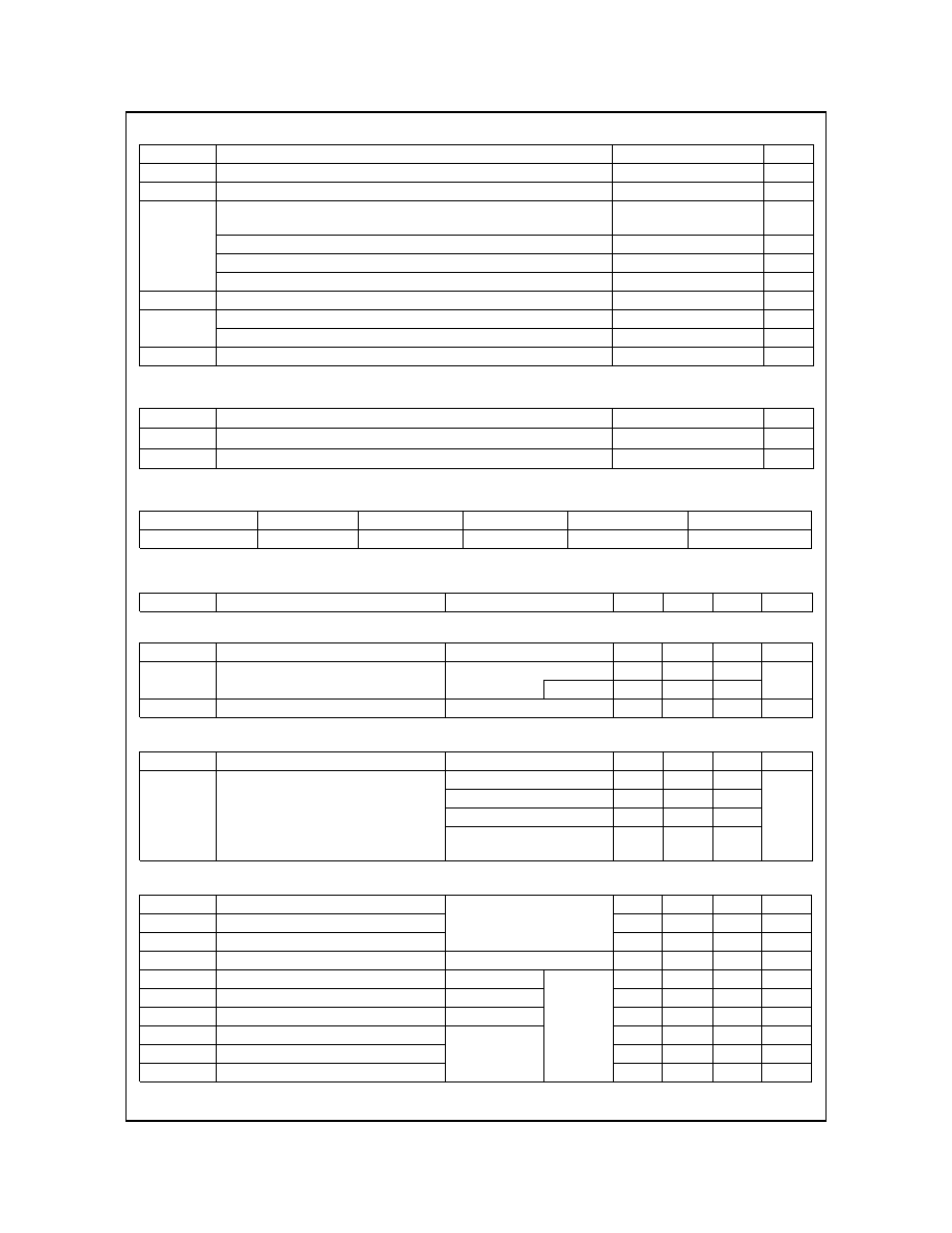
Electrical Characteristics
T
J
= 25°C unless otherwise noted
Symbol
Parameter
Test Conditions
Min
Typ
Max
Units
Off Characteristics
BV
DSS
Drain to Source Breakdown Voltage
I
D
= 1mA, V
GS
= 0V
30
-
-
V
I
DSS
Zero Gate Voltage Drain Current
V
DS
= 24V
V
GS
= 0V
-
-
1
µA
T
J
= 150°C
-
-
250
I
GSS
Gate to Source Leakage Current
V
GS
=
±20V
-
-
±100
nA
On Characteristics
V
GS(th)
Gate to Source Threshold Voltage
V
DS
= V
GS
, I
D
= 250
µA
1
1.7
3
V
R
ON)
Drain to Source On Resistance
I
D
= 80A, V
GS
= 10V
-
1.6
2.3
m
I
D
= 80A, V
GS
= 5V
-
1.9
2.6
I
D
= 80A, V
GS
= 4.5V
-
2.1
2.7
I
D
= 80A, V
GS
= 10V,
T
J
= 175°C
-
2.5
3.6
Dynamic Characteristics
C
ISS
Input Capacitance
V
DS
= 15V, V
GS
= 0V,
f = 1MHz
-
9460
12585
pF
C
OSS
Output Capacitance
-
1710
2275
pF
C
RSS
Reverse Transfer Capacitance
-
1050
1575
pF
R
G
Gate Resistance
f = 1MHz
-
1.8
-
Q
g(TOT)
Total Gate Charge at 10V
V
GS
= 0V to 10V
V
DD
= 15V
I
D
= 80A
I
g
= 1.0mA
-
165
214
nC
Q
g(5)
Total Gate Charge at 5V
V
GS
= 0V to 5V
-
89
115
nC
Q
g(TH)
Threshold Gate Charge
V
GS
= 0V to 1V
-
9.1
12
nC
Q
gs
Gate to Source Gate Charge
-
26
-
nC
Q
gs2
Gate Charge Threshold to Plateau
-
18
-
nC
Q
gd
Gate to Drain "Miller" Charge
-
33
-
nC
DS(
MOSFET Maximum Ratings
T
C
= 25°C unless otherwise noted
Thermal Characteristics
Package Marking and Ordering Information
Symbol
Parameter
Ratings
Units
V
DSS
Drain to Source Voltage
30
V
V
GS
Gate to Source Voltage
±20
V
I
D
Drain Current
Continuous (V
GS
= 10V, T
C
< 163
o
C)
80
A
Continuous (V
GS
= 5V, T
C
< 162
o
C)
80
A
Continuous (V
GS
= 10V, T
C
= 25
o
C, with R
JA
= 43
o
C/W)
31
A
Pulsed
Figure 4
A
E
AS
Single Pulse Avalanche Energy (Note 1)
947
mJ
P
D
Power Dissipation
306
W
Derate above 25
o
C
2.04
W/
o
C
T
J
, T
STG
Operating and Storage Temperature
-55 to +175
o
C
R
JC
Thermal Resistance Junction to Case
0.49
o
C/W
R
JA
Thermal Resistance Junction to Ambient (Note 2)
62
o
C/W
R
JA
Thermal Resistance Junction to Ambient TO-263,1in
2
copper pad area
43
o
C/W
Device Marking
Device
Package
Reel Size
Tape Width
Quantity
FDB8860
FDB8860
TO-263AB
330mm
24mm
800units
FDB8860 N-Channel Logi
c Level
P
o
werTrench
®
MO
SFE
T
FDB8860 Rev A
www.fairchildsemi.com
3
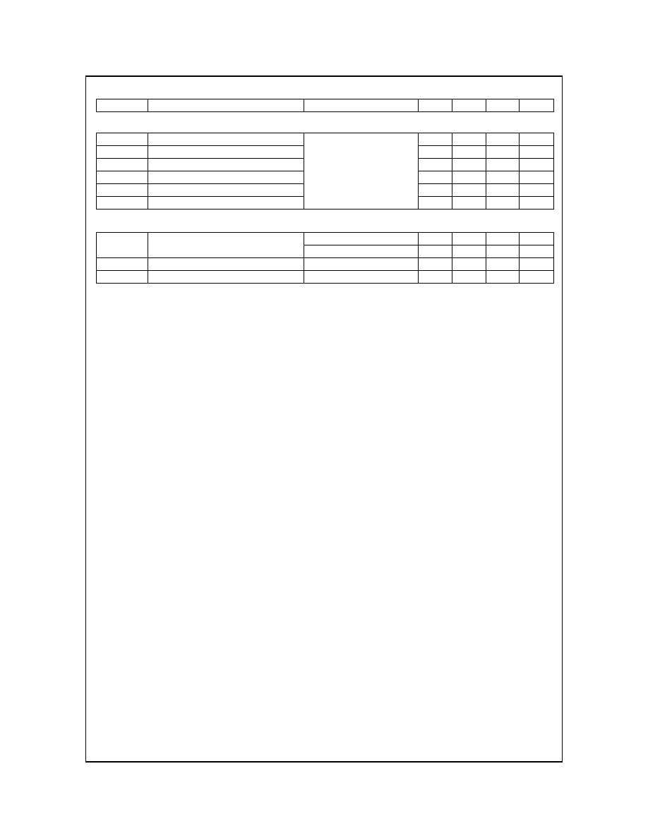
Electrical Characteristics
T
J
= 25°C unless otherwise noted
Switching Characteristics
Drain-Source Diode Characteristics
Symbol
Parameter
Test Conditions
Min
Typ
Max
Units
t
(on)
Turn-On Time
V
DD
= 15V, I
D
= 80A
V
GS
= 5V, R
GS
= 1
-
-
340
ns
t
d(on)
Turn-On Delay Time
-
14
-
ns
t
r
Turn-On Rise Time
-
213
-
ns
t
d(off)
Turn-Off Delay Time
-
79
-
ns
t
f
Turn-Off Fall Time
-
49
-
ns
t
off
Turn-Off Time
-
-
192
ns
V
SD
Source to Drain Diode Voltage
I
SD
= 80A
-
-
1.25
V
I
SD
= 40A
-
-
1.0
V
t
rr
Reverse Recovery Time
I
SD
= 80A, dI
SD
/dt = 100A/
µs
-
-
43
ns
Q
rr
Reverse Recovery Charge
I
SD
= 80A, dI
SD
/dt = 100A/
µs
-
-
29
nC
Notes:
1: Starting T
J
= 25
o
C, L =0.47mH, I
AS
= 64A , V
DD
= 30V, V
GS
= 10V.
2: Pulse width = 100s
This product has been designed to meet the extreme test conditions and environment demanded by the automotive industry. For
a copy of the requirements, see AEC Q101 at: http://www.aecouncil.com/
All Fairchild Semiconductor products are manufactured, assembled and tested under ISO9000 and QS9000 quality systems
certification.
FDB8860 N-Channel Logi
c Level
P
o
werTrench
®
MO
SFE
T
FDB8860 Rev A
www.fairchildsemi.com
4
Typical Characteristics
T
J
= 25°C unless otherwise noted
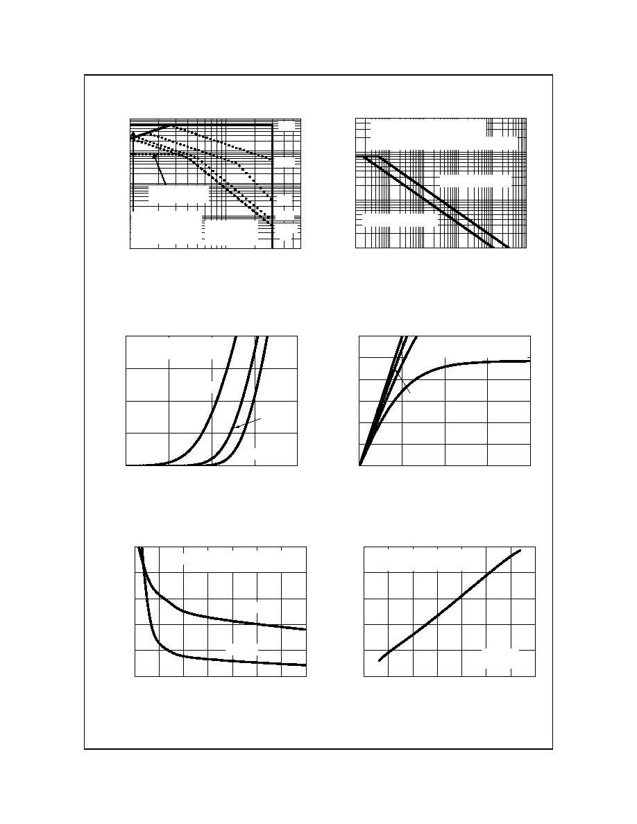
Figure 1. Normalized Power Dissipation vs Case
Temperature
0
25
50
75
100
125
150
175
0.0
0.2
0.4
0.6
0.8
1.0
1.2
PO
W
E
R DI
SS
I
P
ATI
O
N MULI
P
L
I
E
R
T
C
, CASE TEMPERATURE(
o
C)
Figure 2.
25
50
75
100
125
150
175
0
75
150
225
300
V
GS
= 10V
V
GS
= 5V
CURRENT LIMITED
BY PACKAGE
I
D
, D
RAI
N CU
RR
E
N
T
(
A
)
T
C
, CASE TEMPERATURE (
o
C)
Maximum Continuous Drain Current vs
Case Temperature
Figure 3. Normalized Maximum Transient Thermal Impedance
10
-5
10
-4
10
-3
10
-2
10
-1
10
0
10
1
0.01
0.1
1
NOR
M
AL
IZ
ED TH
ERM
A
L
IM
PED
AN
CE Z
JA
t, RECTANGULAR PULSE DURATION (s)
D = 0.5
0.2
0.1
0.05
0.02
0.01
SINGLE PULSE
2
DUTY CYCLE-DESCENDING ORDER
NOTES:
DUTY FACTOR: D = t
1
/t
2
PEAK T
J
= P
DM
x Z
JC
x R
JC
+ T
C
P
DM
t
1
t
2
Figure 4. Peak Current Capability
10
-5
10
-4
10
-3
10
-2
10
-1
10
0
10
1
100
1000
I
(P
K
)
,
P
E
A
K
CU
RRE
N
T
(
A
)
t, PULSE WIDTH (s)
SINGLE PULSE
3000
50
T
C
= 25
o
C
I = I
25
175 - T
C
150
FOR TEMPERATURES
ABOVE 25
o
C DERATE PEAK
CURRENT AS FOLLOWS:
FDB8860 N-Channel Logi
c Level
P
o
werTrench
®
MO
SFE
T
FDB8860 Rev A
www.fairchildsemi.com
5
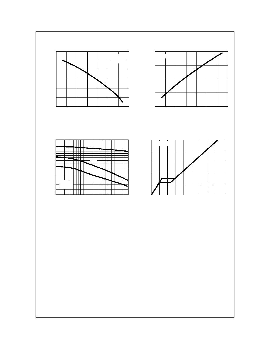
Figure 5.
1
10
0.1
1
10
100
1000
10us
10ms
DC
100ms
1ms
100us
I
D
, DR
AI
N CU
RRE
N
T
(
A
)
V
DS
, DRAIN TO SOURCE VOLTAGE(V)
60
LIMITED BY R
DS(ON)
AREA MAY BE
OPERATION IN THIS
T
C
= 25
o
C
T
J
= MAX RATED
SINGLE PULSE
BY PACKAGE
CURRENT LIMITED
Forward Bias Safe Operating Area
NOTE:
Refer to Fairchild Application Notes AN7514 and AN7515
0.1
1
10
100
1000
10000
1
10
100
STARTING T
J
= 150oC
I AS
, A
V
ALAN
CH
E C
U
R
R
E
NT (A
)
t
AV
, TIME IN AVALANCHE (ms)
STARTING T
J
= 25oC
500
t
AV
= (L)(I
AS
)/(1.3*RATED BV
DSS
- V
DD
)
If R = 0
If R
0
t
AV
= (L/R)ln[(I
AS
*R)/(1.3*RATED BV
DSS
- V
DD
) +1]
Figure 6. Unclamped Inductive Switching
C
apability
Figure 7.
1.5
2.0
2.5
3.0
3.5
0
20
40
60
80
T
J
= -55
o
C
T
J
= 25
o
C
I
D
,
D
RA
I
N
CU
RR
E
NT
(
A)
V
GS
, GATE TO SOURCE VOLTAGE (V)
V
DS
= 7V
T
J
= 175
o
C
PULSE DURATION = 80
µ
s
DUTY CYCLE = 0.5% MAX
Transfer Characteristics
Figure 8.
0.0
0.5
1.0
1.5
2.0
0
20
40
60
80
100
120
V
GS
= 5V
V
GS
= 10V
V
GS
= 4V
PULSE DURATION = 80
µ
s
DUTY CYCLE = 0.5% MAX
I
D
, DR
AIN CU
RR
ENT
(A
)
V
DS
, DRAIN TO SOURCE VOLTAGE (V)
V
GS
= 3V
Saturation Characteristics
Figure 9.
3
4
5
6
7
8
9
10
1.5
2.0
2.5
3.0
3.5
4.0
T
J
= 25
o
C
PULSE DURATION = 80
µ
s
DUTY CYCLE=0.5% MAX
R
DS(
O
N)
,
DRA
IN
TO
S
O
UR
CE
O
N
-RESIST
A
N
C
E
(
m
)
V
GS
, GATE TO SOURCE VOLTAGE (V)
I
D
= 40A
T
J
= 175
o
C
Drain to Source On-Resistance
Variation vs Gate to Source Voltage
Figure 10.
-80
-40
0
40
80
120
160
200
0.6
0.8
1.0
1.2
1.4
1.6
I
D
= 80A
V
GS
= 10V
PULSE DURATION = 80
µ
s
DUTY CYCLE = 0.5% MAX
T
J
, JUNCTION TEMPERATURE(
O
C)
NO
R
M
ALI
Z
E
D
DR
AI
N TO
S
O
URC
E
O
N
-
R
E
S
I
S
T
ANC
E
Normalized Drain to Source On
Resistance vs Junction Temperature
Typical Characteristics
T
J
= 25°C unless otherwise noted
FDB8860 N-Channel Logi
c Level
P
o
werTrench
®
MO
SFE
T
FDB8860 Rev A
www.fairchildsemi.com
6
Figure 11.
-80
-40
0
40
80
120
160
200
0.2
0.4
0.6
0.8
1.0
1.2
1.4
NORM
A
L
IZED
GATE
T
H
RESH
O
L
D VO
LT
A
G
E
T
J
, JUNCTION TEMPERATURE( oC)
V
GS
= V
DS
I
D
= 250
µ
A
Normalized Gate Threshold Voltage vs
Junction Temperature
Figure 12. Normalized Drain to Source
Breakdown Voltage vs Junction Temperature
-80
-40
0
40
80
120
160
200
0.90
0.95
1.00
1.05
1.10
NOR
M
ALIZED
DR
A
I
N
TO S
O
U
RC
E
B
R
EAK
D
O
W
N VO
LT
A
G
E
T
J
, JUNCTION TEMPERATURE(
o
C)
I
D
= 1mA
Figure 13.
0.1
1
10
1000
10000
30
C
rss
C
oss
CAP
ACI
T
AN
CE
(pF)
V
DS
, DRAIN TO SOURCE VOLTAGE (V)
C
iss
f = 1MHz
V
GS
= 0V
500
20000
Capacitance vs Drain to Source
Voltage
Figure 14.
0
20
40
60
80 100 120 140 160 180
0
2
4
6
8
10
I
D
= 1A
V
GS
, G
A
TE
T
O
S
O
UR
CE
V
O
L
T
AG
E
(
V
)
Q
g
, GATE CHARGE (nC)
V
DD
= 15V
I
D
= 80A
Gate Charge vs Gate to Source Voltage
Typical Characteristics
T
J
= 25°C unless otherwise noted

DISCLAIMER
FAIRCHILD SEMICONDUCTOR RESERVES THE RIGHT TO MAKE CHANGES WITHOUT FURTHER NOTICE TO ANY
PRODUCTS HEREIN TO IMPROVE RELIABILITY, FUNCTION OR DESIGN. FAIRCHILD DOES NOT ASSUME ANY LIABILITY
ARISING OUT OF THE APPLICATION OR USE OF ANY PRODUCT OR CIRCUIT DESCRIBED HEREIN; NEITHER DOES IT
CONVEY ANY LICENSE UNDER ITS PATENT RIGHTS, NOR THE RIGHTS OF OTHERS.
TRADEMARKS
The following are registered and unregistered trademarks Fairchild Semiconductor owns or is authorized to use and is
not intended to be an exhaustive list of all such trademarks.
LIFE SUPPORT POLICY
FAIRCHILD'S PRODUCTS ARE NOT AUTHORIZED FOR USE AS CRITICAL COMPONENTS IN LIFE SUPPORT
DEVICES OR SYSTEMS WITHOUT THE EXPRESS WRITTEN APPROVAL OF FAIRCHILD SEMICONDUCTOR CORPORATION.
As used herein:
1. Life support devices or systems are devices or
systems which, (a) are intended for surgical implant into
the body, or (b) support or sustain life, or (c) whose
failure to perform when properly used in accordance
with instructions for use provided in the labeling, can be
reasonably expected to result in significant injury to the
user.
2. A critical component is any component of a life
support device or system whose failure to perform can
be reasonably expected to cause the failure of the life
support device or system, or to affect its safety or
effectiveness.
PRODUCT STATUS DEFINITIONS
Definition of Terms
Datasheet Identification
Product Status
Definition
Advance Information
Preliminary
No Identification Needed
Obsolete
This datasheet contains the design specifications for
product development. Specifications may change in
any manner without notice.
This datasheet contains preliminary data, and
supplementary data will be published at a later date.
Fairchild Semiconductor reserves the right to make
changes at any time without notice in order to improve
design.
This datasheet contains final specifications. Fairchild
Semiconductor reserves the right to make changes at
any time without notice in order to improve design.
This datasheet contains specifications on a product
that has been discontinued by Fairchild semiconductor.
The datasheet is printed for reference information only.
Formative or
In Design
First Production
Full Production
Not In Production
ISOPLANARTM
LittleFETTM
MICROCOUPLERTM
MicroFETTM
MicroPakTM
MICROWIRETM
MSXTM
MSXProTM
OCXTM
OCXProTM
OPTOLOGIC
®
OPTOPLANARTM
PACMANTM
POPTM
Power247TM
PowerEdgeTM
FAST
®
FASTrTM
FPSTM
FRFETTM
GlobalOptoisolatorTM
GTOTM
HiSeCTM
I
2
CTM
i-LoTM
ImpliedDisconnectTM
IntelliMAXTM
Rev. I18
ACExTM
ActiveArrayTM
BottomlessTM
Build it NowTM
CoolFETTM
CROSSVOLTTM
DOMETM
EcoSPARKTM
E
2
CMOSTM
EnSignaTM
FACTTM
FACT Quiet SeriesTM
PowerSaverTM
PowerTrench
®
QFET
®
QSTM
QT OptoelectronicsTM
Quiet SeriesTM
RapidConfigureTM
RapidConnectTM
SerDesTM
ScalarPumpTM
SILENT SWITCHER
®
SMART STARTTM
SPMTM
StealthTM
SuperFETTM
SuperSOTTM-3
SuperSOTTM-6
SuperSOTTM-8
SyncFETTM
TCMTM
TinyLogic
®
TINYOPTOTM
TruTranslationTM
UHCTM
UltraFET
®
UniFETTM
VCXTM
WireTM
Across the board. Around the world.TM
The Power Franchise
®
Programmable Active DroopTM