Äîêóìåíòàöèÿ è îïèñàíèÿ www.docs.chipfind.ru
©2005 Fairchild Semiconductor Corporation
1
www.fairchildsemi.com
FDB33N25 Rev A
FD
B
3
3
N
25
25
0V N
-
C
h
anne
l
M
O
SFE
T
September 2005
UniFET
TM
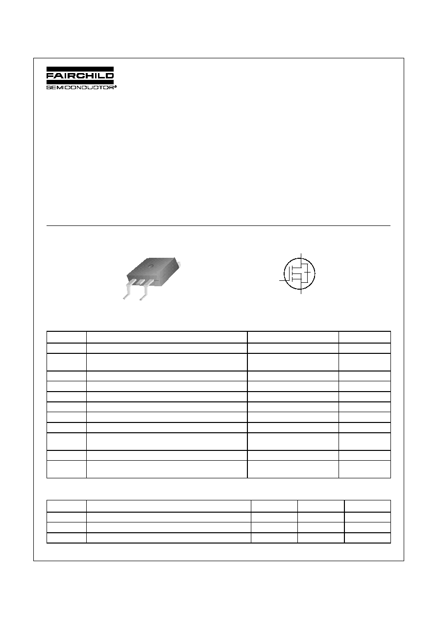
FDB33N25
250V N-Channel MOSFET
Features
· 33A, 250V, R
DS(on)
= 0.094
@V
GS
= 10 V
· Low gate charge ( typical 36.8 nC)
· Low C
rss
( typical 39 pF)
· Fast switching
· 100% avalanche tested
· Improved dv/dt capability
Description
These N-Channel enhancement mode power field effect transis-
tors are produced using Fairchild's proprietary, planar stripe,
DMOS technology.
This advanced technology has been especially tailored to mini-
mize on-state resistance, provide superior switching perfor-
mance, and withstand high energy pulse in the avalanche and
commutation mode. These devices are well suited for high effi-
cient switched mode power supplies and active power factor
correction.
Absolute Maximum Ratings
Thermal Characteristics
S
D
G
G
S
D
Symbol
Parameter
FDB33N25
Unit
V
DSS
Drain-Source Voltage
250
V
I
D
Drain Current
- Continuous (T
C
= 25
°
C)
- Continuous (T
C
= 100
°
C)
33
20.4
A
A
I
DM
Drain Current
- Pulsed
(Note 1)
132
A
V
GSS
Gate-Source voltage
±
30
V
E
AS
Single Pulsed Avalanche Energy
(Note 2)
918
mJ
I
AR
Avalanche Current
(Note 1)
33
A
E
AR
Repetitive Avalanche Energy
(Note 1)
23.5
mJ
dv/dt
Peak Diode Recovery dv/dt
(Note 3)
4.5
V/ns
P
D
Power Dissipation
(T
C
= 25
°
C)
- Derate above 25
°
C
235
1.89
W
W/
°
C
T
J,
T
STG
Operating and Storage Temperature Range
-55 to +150
°
C
T
L
Maximum Lead Temperature for Soldering Purpose,
1/8" from Case for 5 Seconds
300
°
C
Symbol
Parameter
Min.
Max.
Unit
R
JC
Thermal Resistance, Junction-to-Case
--
0.53
°
C/W
R
JA
*
Thermal Resistance, Junction-to-Ambient*
--
40
°
C/W
R
JA
Thermal Resistance, Junction-to-Ambient
--
62.5
°
C/W
* When mounted on the minimum pad size recommended (PCB Mount)
2
www.fairchildsemi.com
FDB33N25 Rev A
FD
B
3
3
N
25
25
0V N
-
C
h
anne
l
M
O
SFE
T
Package Marking and Ordering Information
Electrical Characteristics
T
C
= 25°C unless otherwise noted
NOTES:
1. Repetitive Rating: Pulse width limited by maximum junction temperature
2. L = 1.35mH, I
AS
= 33A, V
DD
= 50V, R
G
= 25
, Starting T
J
= 25
°
C
3. I
SD
33A, di/dt
200A/
µ
s, V
DD
BV
DSS
, Starting T
J
= 25
°
C
4. Pulse Test: Pulse width
300
µ
s, Duty Cycle
2%
5. Essentially Independent of Operating Temperature Typical Characteristics
Device Marking
Device
Package
Reel Size
Tape Width
Quantity
FDB33N25
FDB33N25TM
D2-PAK
330mm
24mm
800
Symbol
Parameter
Conditions
Min.
Typ.
Max Units
Off Characteristics
BV
DSS
Drain-Source Breakdown Voltage
V
GS
= 0V, I
D
= 250
µ
A
250
--
--
V
BV
DSS
/
T
J
Breakdown Voltage Temperature
Coefficient
I
D
= 250
µ
A, Referenced to 25
°
C
--
0.25
--
V/
°
C
I
DSS
Zero Gate Voltage Drain Current
V
DS
= 250V, V
GS
= 0V
V
DS
= 200V, T
C
= 125
°
C
--
--
--
--
1
10
µ
A
µ
A
I
GSSF
Gate-Body Leakage Current, Forward
V
GS
= 30V, V
DS
= 0V
--
--
100
nA
I
GSSR
Gate-Body Leakage Current, Reverse
V
GS
= -30V, V
DS
= 0V
--
--
-100
nA
On Characteristics
V
GS(th)
Gate Threshold Voltage
V
DS
= V
GS
, I
D
= 250
µ
A
3.0
--
5.0
V
R
DS(on)
Static Drain-Source
On-Resistance
V
GS
= 10V, I
D
= 16.5A
--
0.077
0.094
g
FS
Forward Transconductance
V
DS
= 40V, I
D
=16.5A
(Note 4)
--
26.6
--
S
Dynamic Characteristics
C
iss
Input Capacitance
V
DS
= 25V, V
GS
= 0V,
f = 1.0MHz
--
1640
2135
pF
C
oss
Output Capacitance
--
330
430
pF
C
rss
Reverse Transfer Capacitance
--
39
59
pF
Switching Characteristics
t
d(on)
Turn-On Delay Time
V
DD
= 125V, I
D
= 33A
R
G
= 25
(Note 4, 5)
--
35
80
ns
t
r
Turn-On Rise Time
--
230
470
ns
t
d(off)
Turn-Off Delay Time
--
75
160
ns
t
f
Turn-Off Fall Time
--
120
250
ns
Q
g
Total Gate Charge
V
DS
= 200V, I
D
= 33A
V
GS
= 10V
(Note 4, 5)
--
36.8
48
nC
Q
gs
Gate-Source Charge
--
10
--
nC
Q
gd
Gate-Drain Charge
--
17
--
nC
Drain-Source Diode Characteristics and Maximum Ratings
I
S
Maximum Continuous Drain-Source Diode Forward Current
--
--
33
A
I
SM
Maximum Pulsed Drain-Source Diode Forward Current
--
--
132
A
V
SD
Drain-Source Diode Forward Voltage
V
GS
= 0V, I
S
= 33A
--
--
1.4
V
t
rr
Reverse Recovery Time
V
GS
= 0V, I
S
= 33A
dI
F
/dt =100A/
µ
s
(Note 4)
--
220
--
ns
Q
rr
Reverse Recovery Charge
--
1.71
--
µ
C
3
www.fairchildsemi.com
FDB33N25 Rev A
FD
B
3
3
N
25
25
0V N
-
C
h
anne
l
M
O
SFE
T
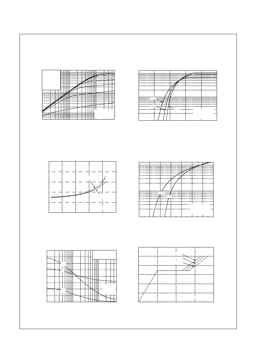
Typical Performance Characteristics
Figure 1. On-Region Characteristics
Figure 2. Transfer Characteristics
Figure 3. On-Resistance Variation vs.
Figure 4. Body Diode Forward Voltage
Drain Current and Gate Voltage
Variation vs. Source Current
and Temperatue
Figure 5. Capacitance Characteristics
Figure 6. Gate Charge Characteristics
2
4
6
8
10
12
10
0
10
1
10
2
150
o
C
25
o
C
-55
o
C
Notes :
1. V
DS
= 40V
2. 250
µ
s Pulse Test
I
D
,
D
r
ai
n C
u
r
r
ent
[
A
]
V
GS
, Gate-Source Voltage [V]
10
-1
10
0
10
1
10
0
10
1
10
2
V
GS
Top : 15.0 V
10.0 V
8.0 V
7.0 V
6.5 V
6.0 V
Bottom : 5.5 V
Notes :
1. 250
µ
s Pulse Test
2. T
C
= 25
I
D
,
Dr
a
i
n
Cu
r
r
e
n
t
[A
]
V
DS
, Drain-Source Voltage [V]
0
20
40
60
80
100
0.00
0.05
0.10
0.15
0.20
0.25
V
GS
= 20V
V
GS
= 10V
Note : T
J
= 25
R
DS
(
O
N
)
[
],
Dra
i
n-S
ourc
e
On-R
esi
s
tance
I
D
, Drain Current [A]
0.2
0.4
0.6
0.8
1.0
1.2
1.4
1.6
10
0
10
1
10
2
150
Notes :
1. V
GS
= 0V
2. 250
µ
s Pulse Test
25
I
DR
, R
e
v
e
rs
e D
r
ai
n C
u
rrent [A
]
V
SD
, Source-Drain voltage [V]
0
10
20
30
40
0
2
4
6
8
10
12
V
DS
= 125V
V
DS
= 50V
V
DS
= 200V
Note : I
D
= 33A
V
GS
,
Ga
t
e
-
S
ou
r
c
e V
o
ltage [V
]
Q
G
, Total Gate Charge [nC]
10
-1
10
0
10
1
0
1000
2000
3000
4000
C
iss
= C
gs
+ C
gd
(C
ds
= shorted)
C
oss
= C
ds
+ C
gd
C
rss
= C
gd
Note ;
1. V
GS
= 0 V
2. f = 1 MHz
C
rss
C
oss
C
iss
Capacitances [pF]
V
DS
, Drain-Source Voltage [V]
4
www.fairchildsemi.com
FDB33N25 Rev A
FD
B
3
3
N
25
25
0V N
-
C
h
anne
l
M
O
SFE
T
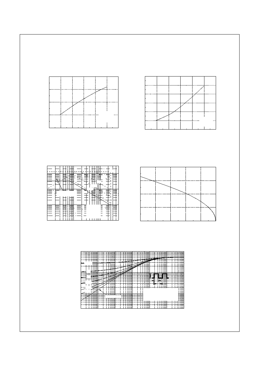
Typical Performance Characteristics
(Continued)
Figure 7. Breakdown Voltage Variation
Figure 8. On-Resistance Variation
vs. Temperature
vs. Temperature
Figure 9. Maximum Safe Operating Area
Figure 10. Maximum Drain Current
vs. Case Temperature
Figure 11. Transient Thermal Response Curve
-100
-50
0
50
100
150
200
0.0
0.5
1.0
1.5
2.0
2.5
3.0
Notes :
1. V
GS
= 10 V
2. I
D
= 16.5 A
R
DS
(
O
N)
,
(
N
or
m
a
l
i
z
ed
)
D
r
ai
n
-
S
o
u
r
c
e
On
-
R
esi
s
t
a
nc
e
T
J
, Junction Temperature [
o
C]
-100
-50
0
50
100
150
200
0.8
0.9
1.0
1.1
1.2
Notes :
1. V
GS
= 0 V
2. I
D
= 250
µ
A
BV
DS
S
, (
N
orm
a
l
i
z
e
d)
D
r
ai
n-S
our
ce B
r
eak
dow
n
V
o
l
t
a
g
e
T
J
, Junction Temperature [
o
C]
25
50
75
100
125
150
0
10
20
30
40
I
D
,
Dr
ai
n Cur
r
e
nt
[
A
]
T
C
, Case Temperature [ ]
10
0
10
1
10
2
10
-1
10
0
10
1
10
2
100 ms
1 ms
10
µ
s
DC
10 ms
100
µ
s
Operation in This Area
is Limited by R
DS(on)
Notes :
1. T
C
= 25
o
C
2. T
J
= 150
o
C
3. Single Pulse
I
D
,
D
r
ai
n C
u
rrent
[A
]
V
DS
, Drain-Source Voltage [V]
1 0
-5
1 0
-4
1 0
-3
1 0
-2
1 0
-1
1 0
0
1 0
1
1 0
-2
1 0
-1
1 0
0
N o te s :
1 . Z
JC
(t) = 0 .5 3
/W M a x.
2 . D u ty F a cto r, D = t
1
/t
2
3 . T
JM
- T
C
= P
D M
* Z
JC
(t)
single pulse
D = 0.5
0.02
0.2
0.05
0.1
0.01
Z
JC
(t
),
Therm
a
l R
e
s
pons
e
t
1
, S q ua re W a ve P u lse D u ra tio n [se c]
t
1
P
DM
t
2
5
www.fairchildsemi.com
FDB33N25 Rev A
FD
B
3
3
N
25
25
0V N
-
C
h
anne
l
M
O
SFE
T
Charge
V
GS
10V
Q
g
Q
gs
Q
gd
3mA
V
GS
DUT
V
DS
300nF
50K
200nF
12V
Same Type
as DUT
Charge
V
GS
10V
Q
g
Q
gs
Q
gd
3mA
V
GS
DUT
V
DS
300nF
50K
200nF
12V
Same Type
as DUT
V
GS
V
DS
10%
90%
t
d(on)
t
r
t
on
t
off
t
d(off)
t
f
V
DD
10V
V
DS
R
L
DUT
R
G
V
GS
V
GS
V
DS
10%
90%
t
d(on)
t
r
t
on
t
off
t
d(off)
t
f
V
DD
10V
V
DS
R
L
DUT
R
G
V
GS
E
AS
=
L I
AS
2
----
2
1
--------------------
BV
DSS
- V
DD
BV
DSS
V
DD
V
DS
BV
DSS
t
p
V
DD
I
AS
V
DS
(t)
I
D
(t)
Time
10V
DUT
R
G
L
I
D
t
p
E
AS
=
L I
AS
2
----
2
1
E
AS
=
L I
AS
2
----
2
1
----
2
1
--------------------
BV
DSS
- V
DD
BV
DSS
V
DD
V
DS
BV
DSS
t
p
V
DD
I
AS
V
DS
(t)
I
D
(t)
Time
10V
DUT
R
G
L
L
I
D
I
D
t
p
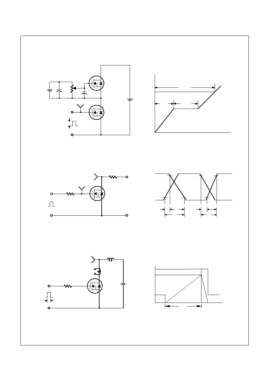
Gate Charge Test Circuit & Waveform
Resistive Switching Test Circuit & Waveforms
Unclamped Inductive Switching Test Circuit & Waveforms
Document Outline