© 2000 Fairchild Semiconductor Corporation
DS009793
www.fairchildsemi.com
October 1988
Revised February 2000
DM9328
Dual
8-
Bit
Shi
f
t
Regi
st
er
DM9328
Dual 8-Bit Shift Register
General Description
The DM9328 is a high speed serial storage element provid-
ing 16 bits of storage in the form of two 8-bit registers. The
multifunctional capability of this device is provided by sev-
eral features: 1) additional gating is provided at the input to
both shift registers so that the input is easily multiplexed
between two sources; 2) the clock of each register may be
provided separately or together; 3) both the true and com-
plementary outputs are provided from each 8-bit register,
and both registers may be master cleared from a common
input.
Ordering Code:
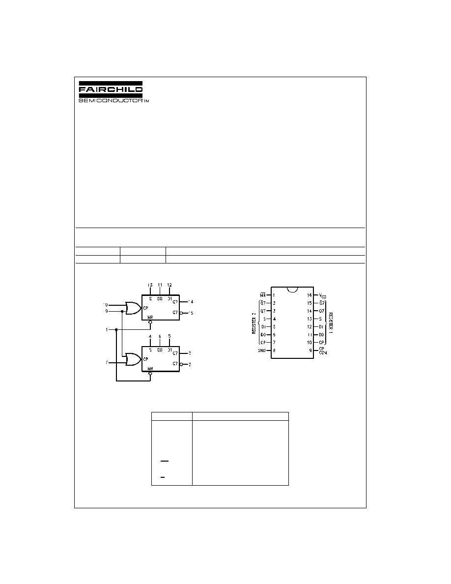
Logic Symbol
V
CC
=
Pin 16
GND
=
Pin 8
Connection Diagram
Pin Descriptions
Order Number
Package Number
Package Description
DM9328N
N16E
16-Lead Plastic Dual-In-Line Package (PDIP), JEDEC MS-001, 0.300 Wide
Pin Names
Description
S
Data Select Input
D0, D1
Data Inputs
CP
Clock Pulse Input (Active HIGH)
Common (Pin 9)
Separate (Pins 7 and 10)
MR
Master Reset Input (Active LOW)
Q7
Last Stage Output
Q7
Complementary Output
www.fairchildsemi.com
2
D
M
9328
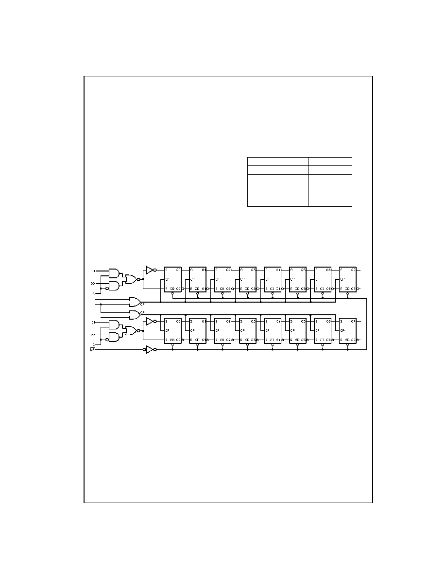
Functional Description
The two 8-bit shift registers have a common clock input
(pin 9) and separate clock inputs (pins 10 and 7). The
clocking of each register is controlled by the OR function of
the separate and the common clock input. Each register is
composed of eight clocked RS master/slave flip-flops and a
number of gates. The clock OR gate drives the eight clock
inputs of the flip-flops in parallel. When the two clock inputs
(the separate and the common) to the OR gate are LOW,
the slave latches are steady, but data can enter the master
latches via the R and S input. During the first LOW-to-
HIGH transition of either, or both simultaneously, of the two
clock inputs, the data inputs (R and S) are inhibited so that
a later change in input data will not affect the master; then
the now trapped information in the master is transferred to
the slave. When the transfer is complete, both the master
and the slave are steady as long as either or both clock
inputs remain HIGH. During the HIGH-to-LOW transition of
the last remaining HIGH clock input, the transfer path from
master to slave is inhibited first, leaving the slave steady in
its present state. The data inputs (R and S) are enabled so
that new data can enter the master. Either of the clock
inputs can be used as clock inhibit inputs by applying a
logic HIGH signal. Each 8-bit shift register has a 2-input
multiplexer in front of the serial data input. The two data
inputs D0 and D1 are controlled by the data select input (S)
following the Boolean expression:
Serial data in: S
D
=
SD0
+
SD1
An asynchronous master reset is provided which, when
activated by a LOW logic level, will clear all 16 stages inde-
pendently of any other input signal.
Shift Select Table
H
=
HIGH Voltage Level
L
=
LOW Voltage Level
X
=
Immaterial
n
+
8
=
indicates state after eight clock pulse
Logic Diagram
INPUTS
OUTPUT
S
D0
D1
Q7 (t
n
+
8
)
L
L
X
L
L
H
X
H
H
X
L
L
H
X
H
H
3
www.fairchildsemi.com
DM9328
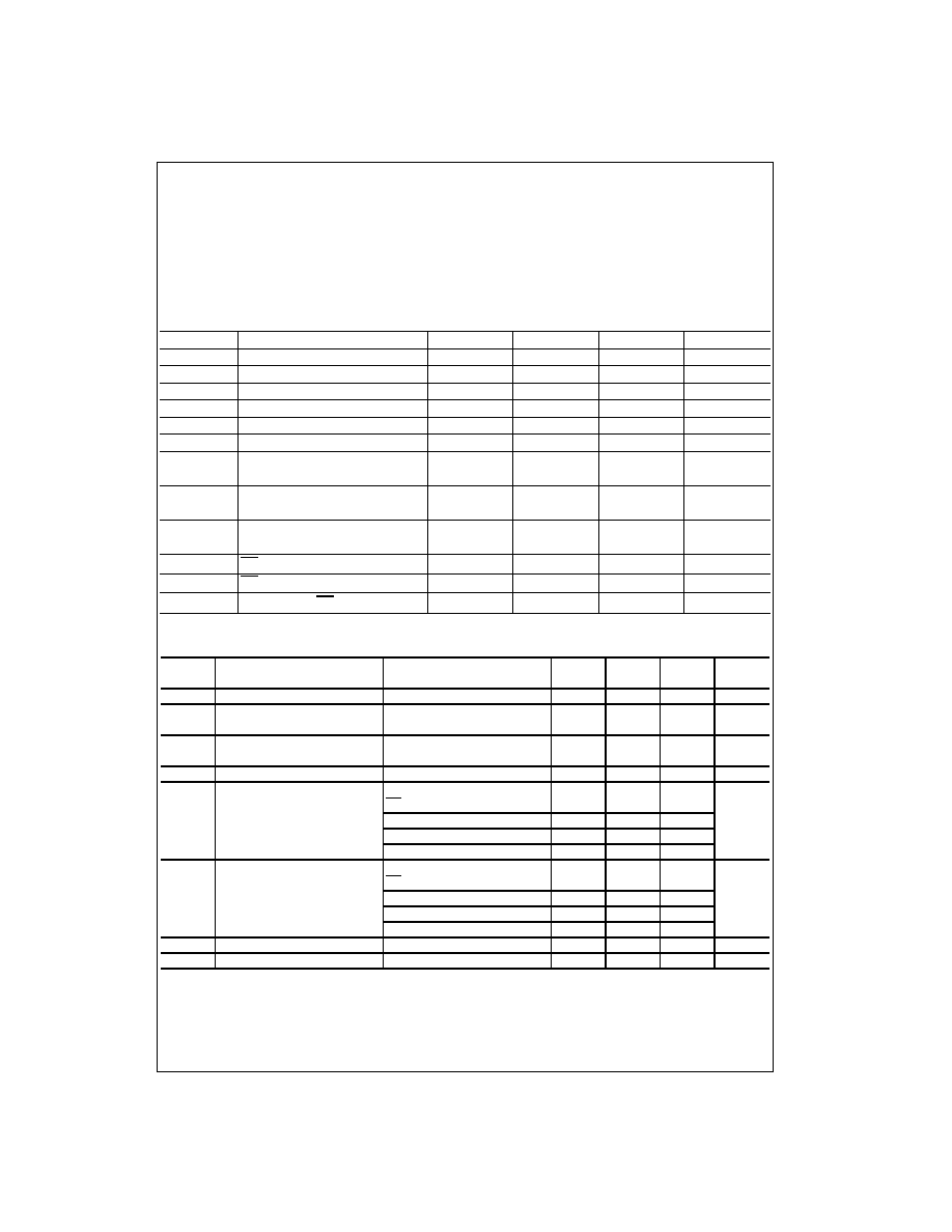
Absolute Maximum Ratings
(Note 1)
Note 1: The "Absolute Maximum Ratings" are those values beyond which
the safety of the device cannot be guaranteed. The device should not be
operated at these limits. The parametric values defined in the "Electrical
Characteristics" table are not guaranteed at the absolute maximum ratings.
The "Recommended Operating Conditions" table will define the conditions
for actual device operation.
Recommended Operating Conditions
Electrical Characteristics
Over Recommended Operating Free Air Temperature Range (Unless Otherwise Noted)
Note 2: All typicals are at V
CC
=
5V, T
A
=
25
°
C.
Note 3: Not more than one output should be shorted at a time.
Supply Voltage
7V
Input Voltage
5.5V
Operating Free Air Temperature Range
0
°
C to
+
70
°
C
Storage Temperature Range
-
65
°
C to
+
150
°
C
Symbol
Parameter
Min
Nom
Max
Units
V
CC
Supply Voltage
4.75
5
5.25
V
V
IH
HIGH Level Input Voltage
2
V
V
IL
LOW Level Input Voltage
0.8
V
I
OH
HIGH Level Output Current
-
0.4
mA
I
OL
LOW Level Output Current
16
mA
T
A
Free Air Operating Temperature
0
70
°
C
t
s
(H)
Setup Time HIGH or LOW
20
ns
t
s
(L)
D
n
to CP
20
t
h
(H)
Hold Time HIGH or LOW
0
ns
t
h
(L)
D
n
to CP
0
t
w
(H)
Clock Pulse Width
25
ns
t
w
(L)
HIGH or LOW
25
t
w
(L)
MR Pulse Width with CP HIGH
30
ns
t
w
(L)
MR Pulse Width with CP LOW
40
ns
t
REC
Recovery Time MR to CP
33
ns
Symbol
Parameter
Conditions
Min
Typ
Max
Units
(Note 2)
V
I
Input Clamp Voltage
V
CC
=
Min, I
I
=
-
12 mA
-
1.5
V
V
OH
HIGH Level
V
CC
=
Min, I
OH
=
Max
2.4
3.4
V
Output Voltage
V
IL
=
Max
V
OL
LOW Level
V
CC
=
Min, I
OL
=
Max
0.2
0.4
V
Output Voltage
V
IH
=
Min
I
I
Input Current @ Max Input Voltage
V
CC
=
Max, V
I
=
5.5V
1
mA
I
IH
HIGH Level
V
CC
=
Max, V
I
=
2.4V
40
Input Current
MR, D
n
Inputs
CP Inputs
60
µ
A
S Inputs
80
CP (COM) Inputs
120
I
IL
LOW Level
V
CC
=
Max, V
I
=
0.4V
-
1.6
Input Current
MR, D
n
Inputs
CP Inputs
-
2.4
mA
S Inputs
-
3.2
CP (COM) Input
-
4.8
I
OS
Short Circuit Output Current
V
CC
=
Max (Note 3)
-
20
-
70
mA
I
CC
Supply Current
V
CC
=
Max
77
mA
www.fairchildsemi.com
4
D
M
9328
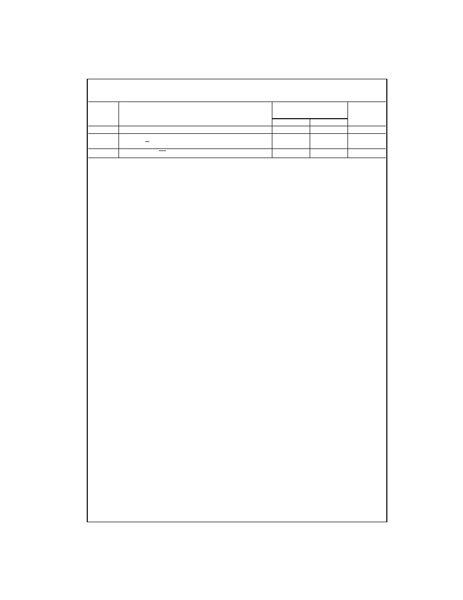
Switching Characteristics
V
CC
=
+
5.0V, T
A
=
+
25
°
C
C
L
=
15 pF
Symbol
Parameter
R
L
=
400
Units
Min
Max
f
MAX
Maximum Shift Right Frequency
20
MHz
t
PLH
Propagation Delay
20
ns
t
PHL
CP to Q7 or Q7
35
t
PHL
Propagation Delay MR to Q7
50
ns
5
www.fairchildsemi.com
DM9328
Dual
8-
Bit
Shi
f
t
Regi
st
er
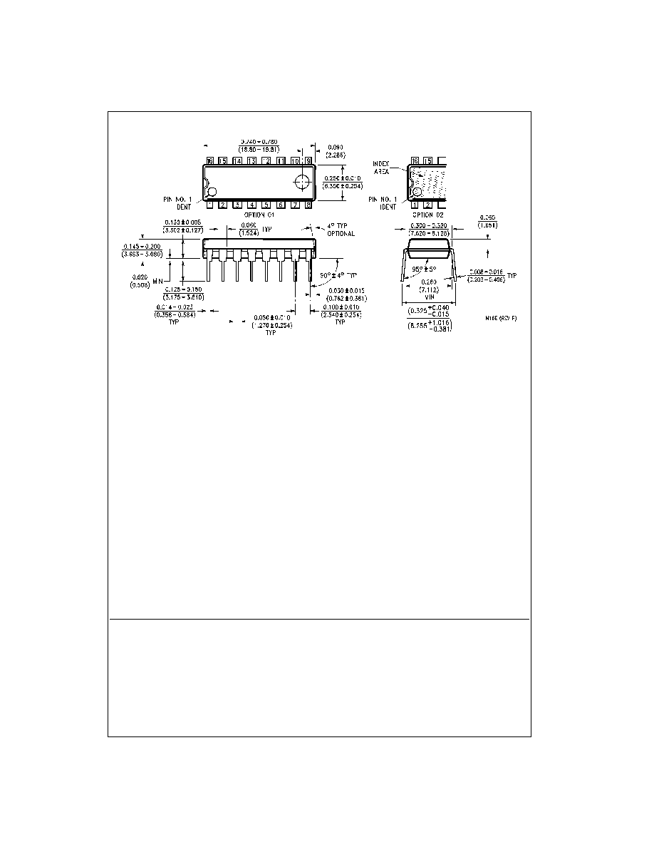
Physical Dimensions
inches (millimeters) unless otherwise noted
16-Lead Plastic Dual-In-Line Package (PDIP), JEDEC MS-001, 0.300 Wide
Package Number N16E
Fairchild does not assume any responsibility for use of any circuitry described, no circuit patent licenses are implied and
Fairchild reserves the right at any time without notice to change said circuitry and specifications.
LIFE SUPPORT POLICY
FAIRCHILD'S PRODUCTS ARE NOT AUTHORIZED FOR USE AS CRITICAL COMPONENTS IN LIFE SUPPORT
DEVICES OR SYSTEMS WITHOUT THE EXPRESS WRITTEN APPROVAL OF THE PRESIDENT OF FAIRCHILD
SEMICONDUCTOR CORPORATION. As used herein:
1. Life support devices or systems are devices or systems
which, (a) are intended for surgical implant into the
body, or (b) support or sustain life, and (c) whose failure
to perform when properly used in accordance with
instructions for use provided in the labeling, can be rea-
sonably expected to result in a significant injury to the
user.
2. A critical component in any component of a life support
device or system whose failure to perform can be rea-
sonably expected to cause the failure of the life support
device or system, or to affect its safety or effectiveness.
www.fairchildsemi.com