Äîêóìåíòàöèÿ è îïèñàíèÿ www.docs.chipfind.ru
©2004 Fairchild Semiconductor Corporation
BZX55C2V4 - BZX55C91, Rev. B1
Zener
s
B
Z
X55
C
2
V
4 -
BZX55C91
Electrical Characteristics
T
A
=25
°
C unless otherwise noted
Device
V
Z
(V) @ I
Z (Note 1)
Z
Z
@ I
Z
(
)
Test Current
I
Z
(mA)
I
R
(
µ
A) @ V
R
I
ZM
(mA)
(Note 2)
Min.
Max.
Ta = 25
°
C
Ta = 125
°
C
V
R
(V)
BZX55C2V4
BZX55C2V7
BZX55C3V0
BZX55C3V3
BZX55C3V6
2.28
2.50
2.8
3.1
3.4
2.56
2.9
3.2
3.5
3.8
85
85
85
85
85
5
5
5
5
5
50
10
4
2
2
100
50
40
40
40
1
1
1
1
1
155
135
125
115
105
BZX55C3V9
BZX55C4V3
BZX55C4V7
BZX55C5V1
BZX55C5V6
3.7
4.0
4.4
4.8
5.2
4.1
4.6
5.0
5.4
6.0
85
75
60
35
25
5
5
5
5
5
2
1
0.5
0.1
0.1
40
40
10
2
2
1
1
1
1
1
95
90
85
80
70
BZX55C6V2
BZX55C6V8
BZX55C7V5
BZX55C8V2
BZX55C9V1
5.8
6.4
7.0
7.7
8.5
6.6
7.2
7.9
8.7
9.6
10
8
7
7
10
5
5
5
5
5
0.1
0.1
0.1
0.1
0.1
2
2
2
2
2
2
3
5
6
7
64
58
53
47
43
BZX55C10
BZX55C11
BZX55C12
BZX55C13
BZX55C15
9.5
10.4
11.4
12.4
13.8
10.6
11.6
12.7
14.1
15.6
15
20
20
26
30
5
5
5
5
5
0.1
0.1
0.1
0.1
0.1
2
2
2
2
2
7.5
8.5
9
10
11
40
36
32
29
27
BZX55C16
BZX55C18
BZX55C20
BZX55C22
BZX55C24
15.3
16.8
18.8
20.8
22.8
17.1
19.1
21.1
23.3
25.6
40
50
55
55
80
5
5
5
5
5
0.1
0.1
0.1
0.1
0.1
2
2
2
2
2
12
14
15
17
18
24
21
20
18
16
BZX55C27
BZX55C30
BZX55C33
BZX55C36
BZX55C39
25.1
28.0
31.0
34.0
37.0
28.9
32.0
35.0
38.0
41.0
80
80
80
80
90
5
5
5
5
2.5
0.1
0.1
0.1
0.1
0.1
2
2
2
2
5
20
22
24
27
28
14
13
12
11
10
Zeners
BZX55C2V4 - BZX55C91
Absolute Maximum Ratings *
T
A
= 25
°
C unless otherwise noted
* These ratings are limiting values above which the serviceability of the diode may be impaired.
Symbol
Parameter
Value
Units
P
D
Power Dissipation
@ TL
75
°
C, Lead Length = 3/8"
500
mW
Derate above 75
°
C
4.0
mW/
°
C
T
J
, T
STG
Operating and Storage Temperature Range
-65 to +200
°
C
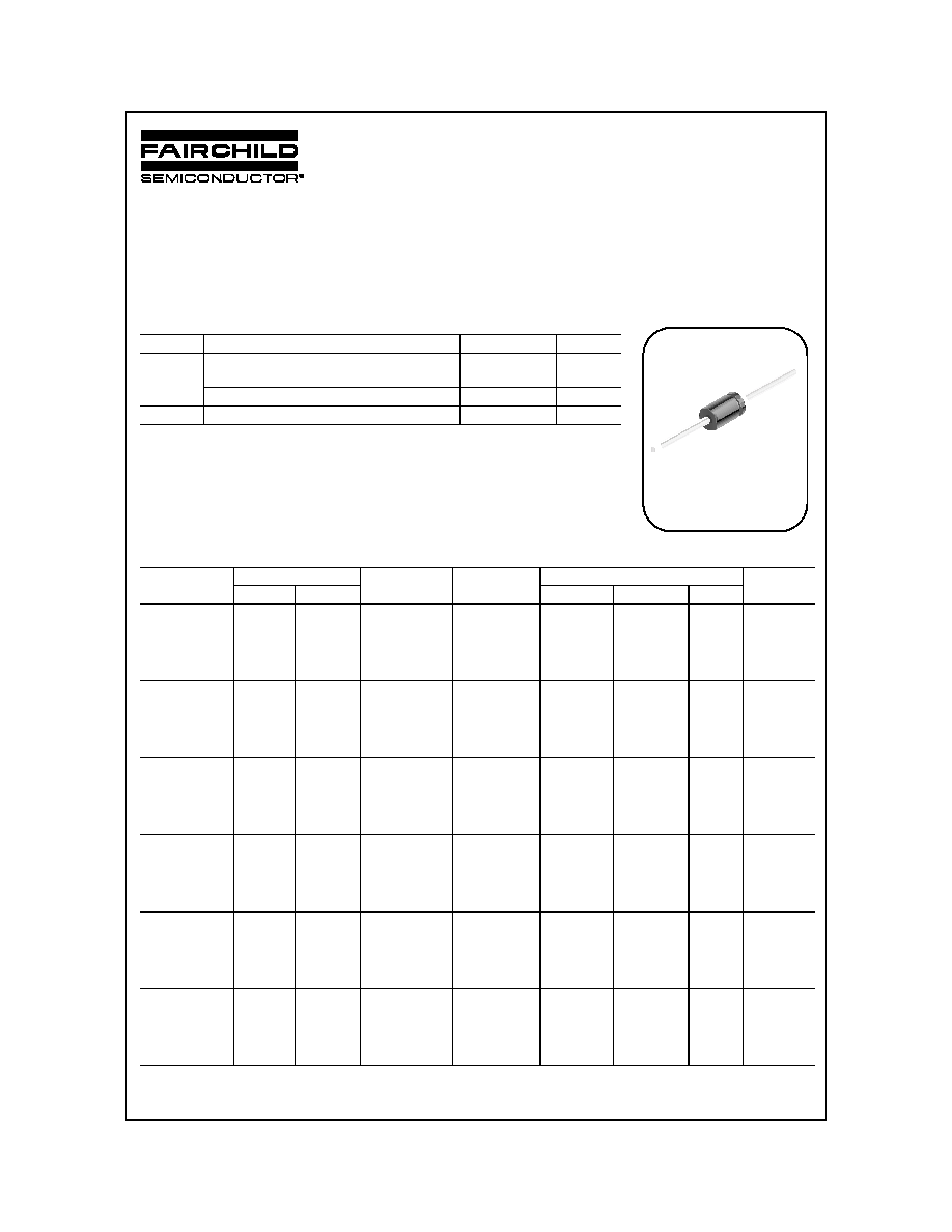
Tolerance = 5%
DO-35 Glass case
COLOR BAND DENOTES CATHODE
©2004 Fairchild Semiconductor Corporation
BZX55C2V4 - BZX55C91, Rev. B1
Zener
s
B
Z
X55
C
2
V
4 -
BZX55C91
Electrical Characteristics
(Continued) T
A
=25
°
C unless otherwise noted
Notes:
1. Zener Voltage (V
Z
)
The zener voltage is measured with the device junction in the thermal equilibrium at the lead temperature (T
L
) at 30
°
C ± 1
°
C and 3/8" lead length.
2. Maximum Zener Current Ratings (I
ZM
)
The maximum current handling capability on a worst case basis is limited by the actual zener voltage at the operation point and the power derating curve.
Device
V
Z
(V) @ I
Z (Note 1)
Z
Z
@ I
Z
(
)
Test Current
I
Z
(mA)
I
R
(
µ
A) @ V
R
I
ZM
(mA)
(Note 2)
Min.
Max.
Ta = 25
°
C
Ta = 125
°
C
V
R
(V)
BZX55C43
BZX55C47
BZX55C51
BZX55C56
BZX55C62
40
44
48
52
58
46
50
54
60
66
90
110
125
135
150
5
2.5
5
5
5
0.1
0.1
0.1
0.1
0.1
5
5
10
10
10
32
35
38
42
47
9.2
8.5
7.8
7.0
6.4
BZX55C68
BZX55C75
BZX55C82
BZX55C91
64
70
77
85
72
80
87
96
160
170
200
250
5
5
5
1
0.1
0.1
0.1
0.1
10
10
10
10
51
56
62
69
5.9
5.3
4.8
4.3
V
F
Forward Voltage = 1.3V Max @ I
F
= 100mA
©2004 Fairchild Semiconductor Corporation
BZX55C2V4 - BZX55C91, Rev. B1
Zener
s
B
Z
X55
C
2
V
4 -
BZX55C91
Top Mark Information
Device
Line 1
Line 2
Line 3
Line 4
BZX55C2V4
BZX55C2V7
BZX55C3V0
BZX55C3V3
BZX55C3V6
LOGO
LOGO
LOGO
LOGO
LOGO
55C
55C
55C
55C
55C
2V4
2V7
3V0
3V3
3V6
XY
XY
XY
XY
XY
BZX55C3V9
BZX55C4V3
BZX55C4V7
BZX55C5V1
BZX55C5V6
LOGO
LOGO
LOGO
LOGO
LOGO
55C
55C
55C
55C
55C
3V9
4V3
4V7
5V1
5V6
XY
XY
XY
XY
XY
BZX55C6V2
BZX55C6V8
BZX55C7V5
BZX55C8V2
BZX55C9V1
LOGO
LOGO
LOGO
LOGO
LOGO
55C
55C
55C
55C
55C
6V2
6V8
7V5
8V2
9V1
XY
XY
XY
XY
XY
BZX55C10
BZX55C11
BZX55C12
BZX55C13
BZX55C15
LOGO
LOGO
LOGO
LOGO
LOGO
55C
55C
55C
55C
55C
10
11
12
13
15
XY
XY
XY
XY
XY
BZX55C16
BZX55C18
BZX55C20
BZX55C22
BZX55C24
LOGO
LOGO
LOGO
LOGO
LOGO
55C
55C
55C
55C
55C
16
18
20
22
24
XY
XY
XY
XY
XY
BZX55C27
BZX55C30
BZX55C33
BZX55C36
BZX55C39
LOGO
LOGO
LOGO
LOGO
LOGO
55C
55C
55C
55C
55C
27
30
33
36
39
XY
XY
XY
XY
XY
BZX55C43
BZX55C47
BZX55C51
BZX55C56
BZX55C62
LOGO
LOGO
LOGO
LOGO
LOGO
55C
55C
55C
55C
55C
43
47
51
56
62
XY
XY
XY
XY
XY
BZX55C68
BZX55C75
BZX55C82
BZX55C91
LOGO
LOGO
LOGO
LOGO
55C
55C
55C
55C
68
75
82
91
XY
XY
XY
XY
©2004 Fairchild Semiconductor Corporation
BZX55C2V4 - BZX55C91, Rev. B1
Zener
s
B
Z
X55
C
2
V
4 -
BZX55C91
Top Mark Information
(Continued)
General Requirements:
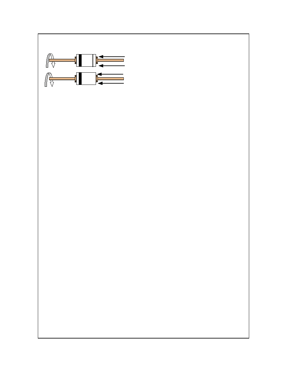
1.0 Cathod Band
2.0 First Line: F - Fairchild Logo
3.0 Second Line: Device name - For 1Nxx series: 3
rd
to 5th characters of the device name.
For BZxx series: 4
th
to 6
th
characters of the device name.
4.0 Third Line: Device name - For 1Nxx series: 6
th
to 7
th
characters of the device name.
For BZXyy series: Voltage rating
5.0 Fourth Line: XY or XYL - Two Digit - Six Weeks Date Code
Where: X represents the last digit of the calendar year
Y represents the Six weeks numeric code
L represents the Large die identification
6.0 Devices shall be marked as required in the device specification (PID or FSC Test Spec).
7.0 Maximum no. of marking lines: 4
8.0 Maximum no. of digits per line: 3
9.0 FSC logo must be 20 % taller than the alphanumeric marking and should occupy the 2 characters of the specified line.
10.0 Marking Font: Arial (Except FSC Logo)
11.0 First character of each marking line must be aligned vertically
F
522
9B
XY
1
st
line: F - Fairchild Logo
2
nd
line: Device Name - 3
rd
to 5
th
characters of the device name.
or 4
th
to 6
th
characters for BZXyy series
3
rd
line: Device Name - 6
th
to 7
th
characters of the device name.
or Voltage rating for BZXyy series
4
th
line: Device Code or - Two Digit - Six Weeks Date Code.
Date code plus or Two Digit - Six Weeks Date Code
Large die identification plus Large die identification, "L"
DISCLAIMER
FAIRCHILD SEMICONDUCTOR RESERVES THE RIGHT TO MAKE CHANGES WITHOUT FURTHER NOTICE TO ANY
PRODUCTS HEREIN TO IMPROVE RELIABILITY, FUNCTION OR DESIGN. FAIRCHILD DOES NOT ASSUME ANY LIABILITY
ARISING OUT OF THE APPLICATION OR USE OF ANY PRODUCT OR CIRCUIT DESCRIBED HEREIN; NEITHER DOES IT
CONVEY ANY LICENSE UNDER ITS PATENT RIGHTS, NOR THE RIGHTS OF OTHERS.
TRADEMARKS
The following are registered and unregistered trademarks Fairchild Semiconductor owns or is authorized to use and is
not intended to be an exhaustive list of all such trademarks.
LIFE SUPPORT POLICY
FAIRCHILD'S PRODUCTS ARE NOT AUTHORIZED FOR USE AS CRITICAL COMPONENTS IN LIFE SUPPORT
DEVICES OR SYSTEMS WITHOUT THE EXPRESS WRITTEN APPROVAL OF FAIRCHILD SEMICONDUCTOR CORPORATION.
As used herein:
1. Life support devices or systems are devices or
systems which, (a) are intended for surgical implant into
the body, or (b) support or sustain life, or (c) whose
failure to perform when properly used in accordance
with instructions for use provided in the labeling, can be
reasonably expected to result in significant injury to the
user.
2. A critical component is any component of a life
support device or system whose failure to perform can
be reasonably expected to cause the failure of the life
support device or system, or to affect its safety or
effectiveness.
PRODUCT STATUS DEFINITIONS
Definition of Terms
Datasheet Identification
Product Status
Definition
Advance Information
Preliminary
No Identification Needed
Obsolete
This datasheet contains the design specifications for
product development. Specifications may change in
any manner without notice.
This datasheet contains preliminary data, and
supplementary data will be published at a later date.
Fairchild Semiconductor reserves the right to make
changes at any time without notice in order to improve
design.
This datasheet contains final specifications. Fairchild
Semiconductor reserves the right to make changes at
any time without notice in order to improve design.
This datasheet contains specifications on a product
that has been discontinued by Fairchild semiconductor.
The datasheet is printed for reference information only.
Formative or
In Design
First Production
Full Production
Not In Production
ImpliedDisconnectTM
ISOPLANARTM
LittleFETTM
MICROCOUPLERTM
MicroFETTM
MicroPakTM
MICROWIRETM
MSXTM
MSXProTM
OCXTM
OCXProTM
OPTOLOGIC
OPTOPLANARTM
FACT Quiet SeriesTM
FAST
FASTrTM
FPSTM
FRFETTM
GlobalOptoisolatorTM
GTOTM
HiSeCTM
I
2
CTM
i-LoTM
Rev. I10
ACExTM
ActiveArrayTM
BottomlessTM
CoolFETTM
CROSSVOLTTM
DOMETM
EcoSPARKTM
E
2
CMOSTM
EnSignaTM
FACTTM
PACMANTM
POPTM
Power247TM
PowerSaverTM
PowerTrench
QFET
QSTM
QT OptoelectronicsTM
Quiet SeriesTM
RapidConfigureTM
RapidConnectTM
SILENT SWITCHER
SMART STARTTM
SPMTM
StealthTM
SuperFETTM
SuperSOTTM-3
SuperSOTTM-6
SuperSOTTM-8
SyncFETTM
TinyLogic
TINYOPTOTM
TruTranslationTM
UHCTM
UltraFET
VCXTM
Across the board. Around the world.TM
The Power Franchise
Programmable Active DroopTM